 |
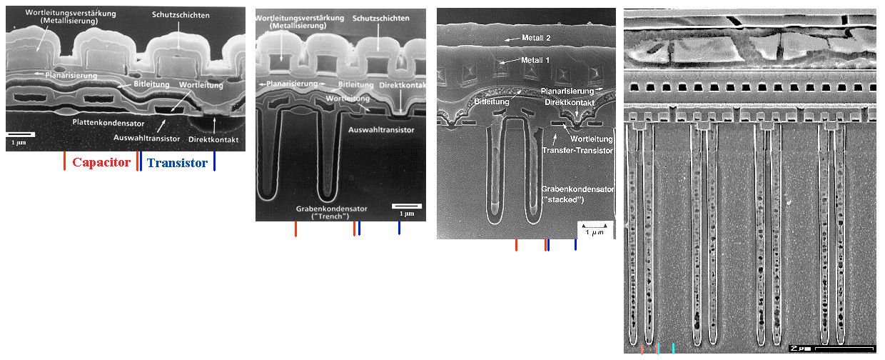
It is quite instructive, if difficult to arrange, to look at several generations of DRAMs in direct comparison. |
|
 |
The picture below shows cross sections though the transistor - capacitor region
necessary to store 1 bit - from the 1 Mbit DRAM to the 64 Mbit DRAM (all of Siemens
design) |
|
 |
The pictures have been scaled to about the same magnification; the assembly is necessarily
quite large. It starts with the 1 Mbit DRAM on the left, followed by the 4 Mbit, 16 Mbit and 64
Mbit memory. |
| |
|
 |
Decrease in feature
size and some new key technologies are easily perceived. Most prominent
are: |
|
 |
Planar capacitor ("Plattenkondensator")
for the 1 Mbit DRAM; LOCOS isolation and 1 level of metal ("Wortleitungsverstärkung")
parallel to the poly-Si "Bitleitung" (bitline) and at right angles to the poly-Si/Mo-silicide "Wortleitung"
(wordline). |
|
 |
Trench capacitor for the 4 Mbit DRAM, "FOBIC"
contact, and TiN diffusion barrier. |
|
 |
Two metal levels for the 16 Mbit DRAM, poly-ONO-poly
in trench; improved planarization between bitline - metal 1, and metal 1 - metal 2. |
|
 |
Box isolation instead of LOCOS for the 64 Mbit DRAM, very deep trenches, W-plugs,
and especially complete planarization with chemical mechanical polishing
(CMP),
the key process of supreme importance for the 64 Mbit generation and beyond. |
 |
If some of the technical expressions eluded you - don`t worry, be happy! We
will get to them quickly enough. |
 |
Parallel to a reduction in feature size is always an increase in chip size; this is illustrated the link. |
|
 |
You may ask yourself: Why do we not just make the chip bigger - instead of 200
4 Mbit DRAMs on a wafer we just as well produce 50 16 Mbit Drams? |
|
 |
Well. Le's say you have a very high yield of
75 % in your 4 Mbit production. This gives you 150 good chips out of your 200 - but it would
give you a yield close to zero if you now make 16 Mbit DRAMs with that technology. |
|
 |
What's more: Even if you solve the yield problem: Your 16 Mbit chips would be exactly
4 times more expensive then your 4 Mbit chip - after all your costs have not changed and you now produce only
a quarter of what you had before. Your customer would have no reason to buy these chips, because they are not only not cheaper
per bit, but also not faster or less energy consuming. |
|
 |
Progress performance only can come from reducing the feature size. |
 |
The cost per bit problem you also can address to some extent by using larger wafers,
making more chips per process run. |
|
 |
This has been done and is being done: Wafer sizes increased from < 2 inch in the
beginning of the seventies to 300 mm now (2002) - we also went metric on the way. |
© H. Föll (Electronic Materials - Script)
