 |
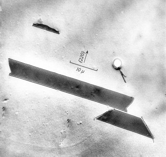
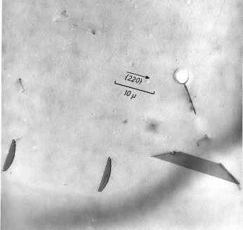
Shown is the same area of a Si sample imaged with two different diffraction
vectors of the {220} type. The defects are the result of an epitaxial
process used for making integrated circuits
which was followed by diffusion /oxidation step. |
|
 |
Whereas some defects completely vanish with one diffraction vector and show strong contrast
with the other one, the medium sized defects stay in contrast (the small dislocation ending at an etch pit, too). |
| |
| |
|
|
 |
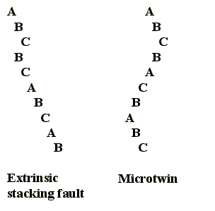
Further analysis, using more special diffraction conditions, show the that medium
sized defect is a micro twin. The difference between micro twins and stacking faults is shown in the graphic below: |
| |
|
|
|
|
 |
An interesting side observation was that the microtwins "killed" the devices, while
the stacking faults did not. In other words, devices containing stacking faults still worked, while the ones with a microtwin
inside were electrically faulty. |
 |
This is a correlation that cannot be obtained by defect etching or any method without "high
resolution", because a microtwin and a stacking faults would be indistinguishable. |
| | |
| |
© H. Föll (Defects - Script)


![]() 6.1.1 Observation of Dislocations and Other Defects
6.1.1 Observation of Dislocations and Other Defects ![]() 6.3.3 Stacking Faults and Other Defects
6.3.3 Stacking Faults and Other Defects