5.3 Pore Etching | ||||
5.3.1. Introduction | ||||
![]() |
All the fooling around with electrochemical etching produced some strange stuff
besides the wanted defect delineation. Somewhat simplified we had:
| |||
| ||||
![]() |
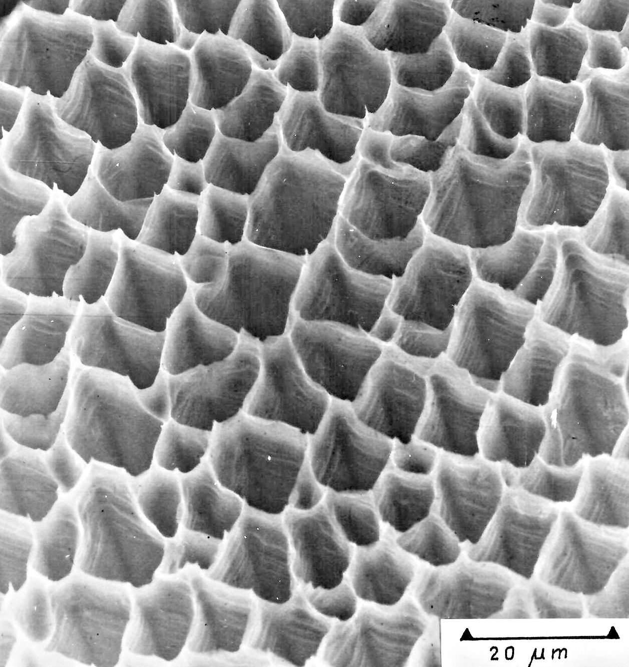
That is a SEM picture of an utterly black surface. Take n-type -Si and etch it
anodically while illuminating the front-side and that is what you might get. It was quite puzzling but the pictures made
clear why the silicon surface was now pitch-black. I came up with an explanation for this kind of pore etching: The bending of the space charge region around some depression would focus the holes generated by the light on the tip of the depression, thus strengthening dissolution at the tip region. Based on this I made a prediction: Illuminate the back side of n-Si with a large diffusion length (comparable to the specimen thickness) and you are going to produce deep pore. Volker Lehmann went to work. The result was this publication: | |||
60 | V. LEHMANN, V. , FÖLL, H.: Formation mechanism and properties of electrochemically etched trenches in n-type silicon. J. Electrochem. Soc., 137 (1990) 653 (1 133 citations) | |||
![]() |
This paper got 1 154 citations (April 2023)! !
This is my most cited paper! It opened a rather wide field of research: Electrochemically etched pores of all kinds in semiconductors
of all kinds. Many more (> 100) publications dealing with pores in semiconductors with my name on it were to follow.
Volker Lehmannm however, did even better. After I left Siemens, he spend some time with my very good friend Uli Gösele, then at Duke University, USA: There he encountered the magic word "nanowire" and with his background of investigating those colorful layers on anodized Si, it was all that was needed to produce this publication: | |||
![]() |
V Lehmann, U Gösele:: Porous silicon formation: A quantum wire effect V
Applied Physics Letters, 1991 2682 citations! Can't do much better than that as long as your first name is not Albert. Well - the referee (of course) strongly opposed publication; look it up here. I know about that because Volker was a bit shocked after getting the referee report and asked for my advice. |
|||
5.3.2 Publications | ||
![]() |
Well, there is the major publication given above. Then there is just one more produced during my Siemens time: | |
67 | FÖLL;
H.: Properties of silicon-electrolyte junctions and their application to silicon characterization. Appl. Phys. A 53
(1991) 8 - 19 (236 citations) This article actually constitutes the first review of the peculiarities of Si electrochemistry and contains macropore etching. I wrote it while still at Siemens but ready for going to Kiel This article was actually dedicated to H.-J. Queisser on the occasion of his 60th birthday. Prof. Queisser was a kind of mentor to me, helping me along in my career every now and then and Im pleased that this article was quite well received. | |
![]() |
That's all there is for my Siemens time. However, some 100+ publications about pore etching in semiconductors were to follow during my time in Kiel. |
5.3.3 Pictures |
||||
![]() |
Pore etching pictures are mostly from a SEM, i.e. produced by a scanned beam and nowadays intrinsically digital. However, in those long forgotten days around 1990, what you got was still a photograph of the (analog) picture as seen on an screen. Typically done with a Polaroid camera, producing an (almost) instant picture and, if so desired, a negative. This is why I still give you a few originals here. Just a few, mostly relating to the publication, since I dont have others anymore. | |||
| ||||
![]() |
![]() |
![]() |
![]() |
© H. Föll (Archive H. Föll)