| | 5.2 ELYMAT |
| |
5.2.1 Introduction |
 |
Playing around with the electrochemistry of silicon in the context of characterizing
rather outlandish Si samples had some major far-reaching consequences: It would dominate a large part of my future research
interests. Even better, it also dominated the research interest of V. Lehmann and, up to a point, U. Gösele. It would
also be fair to say that it influenced the research of quit e a few other scientists; witness the biannual “PSST”,
an international conference dedicated to porous semiconductors science and technology.
In essence, Volker Lehamnn and
I, playing around with electrochemistry for fun, not for what we were paid to do, contributed (a lot!), then and later,
to these four topics:
- The “ELYMAT”, short for ELectrolYtical MetAl Tracing;
- Macropore etching in n-type silicon via back-side illumination;
- Nanoporous” silicon, in particular recognizing what it is;
- Mysteries of semiconductor electrochemistry, in particular self-organization
phenomena like current / voltage oscillations.
|
|
 |
The first two items resulted from figuring out that minority carriers in standard
wafers made for microelectronics had diffusion lengths in the order of the wafer thickness. Producing an excess of minority
carriers close to one surface by illumination thus would also increase the concentration at the other side since the carriers
could diffuse that far.
One could use these carriers in two ways:
- Generate electrons by a scanned Laser beam on the front side of a p-type wafer and measure how many of them made it
to the backside by simply de-coupling them as leakage current at an electrolyte junction. This allowed a rather simple and
direct measurement of the diffusion length and thus enabled diffusion length mapping.
That is the principle of the ELYMAT, covered here.
- Holes produced by globally illuminating the backside of n-type wafers would diffuse to the front side where they would
be focused on small depressions by the electrical field produced by biasing the system in an electrolytic cell. This restricted
electrochemical dissolution to the bottom of the pits and produced macropores with large
aspect ratios,
|
 |
Macropores will be the topic of the next module; here we look at
the ELYMAQT. |
| | |
|
| 5.2.2. Publications
|
 |
The ELYMAT, now long since forgotten, actually made it to a commercial product,marketed
by the conpany GeMeTec. That is a rather rarer event for something coming out of rather basic research and that’s why
I supply a short history here.
This archive is mostly about preserving
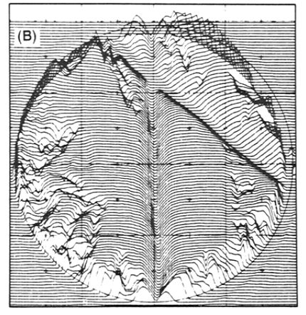
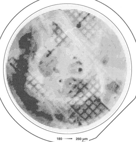
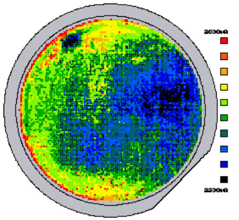
high-quality pictures. I’m sorry to say that there aren’t any from the ELYMAT. One could expect some colorful
maps of the lifetime and the like but this couldn’t be done back in the 1980ties! There were no PCs around yet and
the storage media of choice was thee floppy disc, barely holding about 1 MB of data (i.e. one color picture). Cheap color
printers were a dream at best. I can’t do much better than the publications and thus supply very little in what follows. |
|
 |
Not counting minor proceedings, we have the following publications (including
the ones from the Kiel time): |
| |
58 |
LEHMANN, V.,
FÖLL, H.: Minority carrier diffusion length mapping in silicon wafers using a Si-electrolyte-contact. J. Electrochem.
Soc., 135 (1988) 2831 E (155 citation
That is tie first publication intriducing the method. |
| |
63 |
FÖLL. H., LEHMANN, V., ZOTH, G., GELSDORF, F., GÖTTINGER, B.: In-line
monitoring of heavy metal contaminations and interface states by an imaging technique. Proc. of the Satellite Symposium
to ESSDERC '89 Berlin. (Analytical Technique for Semiconductor Material and Process Characterization) (eds.: B.O. Kolbesen,
D.V.Mc Caughan, W. Wandervorst) Electrochem. Soc. Proc. Vol. 90-11 (1990) 44 (invited paper) |
| | 71 |
FÖLL, H.: Life time mapping with the ELYMAT technique. Proc. Symp. "Advanced
Science and Technology of Si Materials", (Jap. Soc. Promotion of Science) Kona (Hawaii) 1991, p. 347 (invited paper)
3 citations) |
| |
74 |
FÖLL, H., LEHMANN, V., LIPPIK, W.: Characterization of single and polycrystalline
silicon by extension of the ELYMAT technique. Proc. of the Satellite Symp. to ESSDERC '93 Grenoble, "Crystalline Defects
and Contamination: Their Impact and Control in Device Manufacturing", (ECS Proc. Vol. 93-15, 1993), p. 252
First
time that Wolfgang
Lippik appears, my first Ph.D studnet who not only did the ELYMAT work in KIel but taught me HTML so I could
write all those Hyerscripts. |
| |
73 |
CARSTENSEN, J., LIPPIK, W., FÖLL, H.: Mapping of defect related bulk and
surface properties with the ELYMAT technique. In Semiconductor Silicon/1994 (eds, H.R. Huff, W. Bergholz, K. Sumino),( ECS
Proc. Vol. 94-10), San Francisco 1994, p. 1105 (8 citations)
First time the name Jürgen Carstensen appears. He
was a theoretical physicist, just finished with his Ph.D thesis and he joined my group to stay. He was the second in command
of my group ever since and |
| |
76 |
CARSTENSEN, J., LIPPIK, W., FÖLL, H.: Mapping of defect related silicon
properties with the ELYMAT technique in three dimensions. Proc. of "Semiconductor Processing and Characterization with
Laser-Applications in Photovoltaics", Stuttgart 1994, Mat. Science Res. Forum Vols. 173-174, p.159 5
citations) |
| |
78 |
CARSTENSEN, J., LIPPIK, W., LIEBERT, S., KÖSTER, S., FÖLL, H.: New
developments of the ELYMAT technique. Proc. of the Satellite Symp. to ESSDERC '95 Den Haag, "Analytical Techniques
for Semiconductor Materials and Process Characterisation II", Electrochem.Soc. Proc. Vol. 95-30 (1995) 83-92 |
| | 79
|
CARSTENSEN, J., LIPPIK, W., LIEBERT, S., KÖSTER, S., FÖLL, H.: ELYMAT
technique on multicrystalline silicon for solar cell application.. Proc. of the "13th European Photovoltaic Conference
and Exhibition", Nice, Okt. 1995, p. 1344-1347 2 citations) |
| | |
|
© H. Föll (Archive H. Föll)


