Pictures to: 3.3.1 Defects in EFG Si Ribbons

The first few pictures relate to the ones mentioned in the report. They are not complete – I do not have anything left from the
defect etching and just one picture from the EBIC work.
   
 
Defects in EFG ribbons
Similar to Fig 8 in the report.
Note: At the time this picture was taken, there may have been 5 electron microscopes capable of producing HRTEM
“lattice imaging” pictures, and just a handful of electron microscopists capable of pushing the TEM to these limits.
The picture above showing twin boundaries is among the very early HRTEM pictures; it may well be the first on
showing twin boundaries. It never occurred to me to publish results like this. After all, you just could see that a
twin boundary looks exactly as it must. Nothing new about this, Same things for defects like stacking faults.
You can tell that I was not an American. They perceived thing differently. Researchers from Bell Labs (No. 1
research institution of the world then) came to Cornell university to use “my” microscope to do HRTEM work
and then published a (trivial, in my eyes) picture of a stacking fault. I had already a whole collection of HRTEM
images (some shown below) but never considered to publish the stuff just so.
 
Defects in EFG ribbon
Fig. 9 in report.
This was actually a puzzling picture. On the fist look the grayish thing appears to be grain boundary but then grain boundaries
cannot end ion the crystal. It’s actually a micro twin but you had to know about these special defects to understand what you saw.
Once more, due to the work with integrated circuits, I knew about this Si speciality
 
Defects in EFG ribbons; HRTEM
Fig. 10 in report
This is a very special picture; I will have more to say further down.
 
Defects in EFG ribbons
Fig. 11 in report.
We see microtwins "edge on" that end in some "planar defect". Despite extensive
contrast analysis, I couuld not figure out what those planar defects are
 
Defects in EFG ribbons
Fig. 12 in report.
Essentially a low-angle grain boundary.
 
EBIC defects in Si ribbons
Related to Fig. 7 in report
The only EBIV picture still around. That clean twin boundaries cannot be electrically active
is well understood by now.
 
Defects in EFG ribbons
Auxiliary picture showing an assembly of microtwins.
It is clear by now that plastic deformation of Si (at higher temperatures) involves a lot of twinning
I'm not sure if this is fully understood
 
Defects in EFG ribbons
Auxiliary figure.
Showing the "meeting" of 3 grain boundaries and a "Bollmamnn" structure within one of therm.
 
Defects in EFG ribbons
Auxiliary picture.
We see how an external dislocations end in grain boundary and is accommodated
by a re-arrangement of the "Bollmann" dislocations in the boundary
 
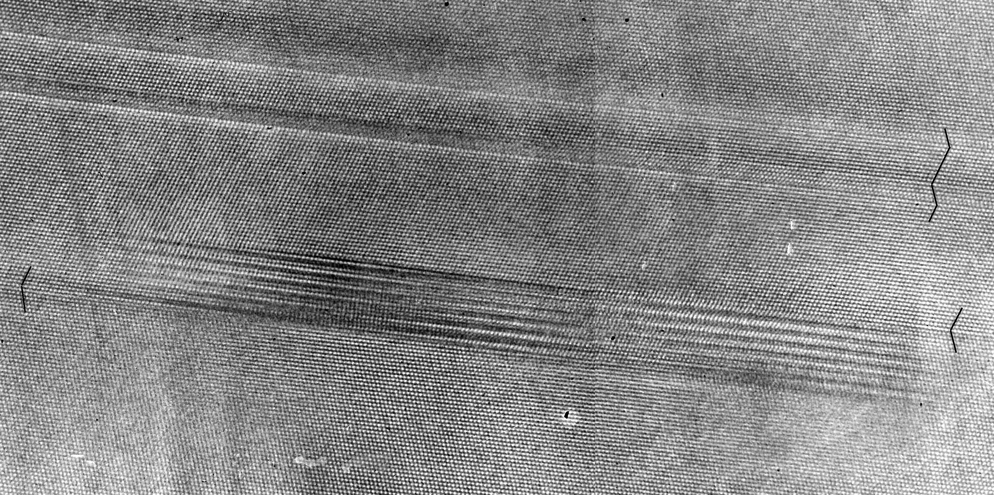
Defects in EFG ribbons; HRTEM
Same as Fig. 10 in the report.
Scanned form a large scale print in two parts and "glued" together.
That is a very special picture. I fondly believe that it is the first HRTEM picture of a non-trivial defect in Si. The “striped” structure is an incoherent twin boundary.
Still rather trivial but a notch above simple stacking faults and coherent twin boundaries. We see about 60 % of the negative area. We also see it with optimized contrast.
The negative actually had too much contrast on a large scale, i.e. some parts were rather bright and others dark. The way to to deal with that in the old days of yore
was to produce a de-focussed positive of the negative that blurred the details but kept the large scale contrast. Then you superimpose this positive on the original
negative, i.e. where the original negative was very bright you had dark regions in the positive and vice verse. Thusly you evened out the large scale brightness variations.
From the (physically, took some precision work) superimposed negative / positive combinations you produced a new negative that now was rather homogeneous
in the over.-all brightens (took some experimenting with various positives). Of course this negative also lost some of the short range contrast which you tried to
counter by printing on “hard” paper. Altogether you spent many hours in the dark room. The result, however, was worth it! 
I never published sixths picture because the reductions in size necessary for any journal would make it impossible to see anything.
D. Ast, my advisor then, later published it in one of his articles and – surprise! - you don’t see anything.
 
Defects in EFG ribbons; HRTEM
Auxiliary picture.
Just for good measure: HRTEM of "trivial" twin boundaries in silicon

With frame With frame as PDF

go to 3.3 Defects in EFG Si Ribbons

© H. Föll (Archive H. Föll)