| |
3.3 Defects in EFG Si Ribbons |
| | 3.3.1 Background |
 |
Nov. 25th 1973 is a day to remember. It was a Sunday and you were forbidden to
drive your car on a German “Autobahn”! We experienced the high point of the first (world-wide) oil crisis! The
crisis started the very first wave of research in what today we like to call “green” energies, in particular solar
energy and solar cells. My post-doc contract with Cornell university included TEM studies in Si ribbons made by the “Edge-defined Film fed Growth” (EFG) method. I actuality did a lot
of work on this topic – but never published anything! |
|
 |
Nevertheless; I include some pictures and explanations here for a very good reason: |
| | |
|
| |
|
This work started me on solar cell research
|
|
| | |
|
| |
|
Since 1977 until 2014 when I retired, I have worked almost without interruptions
on solar cell research. |
| |
| |
|
 |
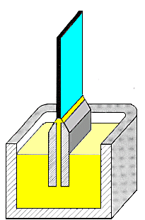
What is "Edge-defined Film fed Growth"? Well, it was one of the many
(mostly apparently crazy) methods to come up with thin sheets or ribbons of solar-grade silicon that could be used directly
to make good solar cells. The picture on the right gives an idea of how to pull a Si ribbon with the help of a die. Use this link if you want to know more.
Two points should be made today (Nov. 2022)
| |
 | | Pulling an EFG ribbon from a die |
|
| |
1 |
None of these (and lots of other methods / materials) made it. Solar cells today are the
cheapest way to produce electrical energy (something none of us would have believed in 1977), and they are mad by cutting
Si “wafers” (typically square) from blocks of cast silicon. All these many methods that wanted to avoid the expensive
and wasteful cutting process added costs and waste of their own and did not anticipate that cutting would become very cheep
(by using wire saws that cut 100 wafers in parallel) and produce almost no waste anymore (by using ultra-thin wires).
You also can't beat silicon pricewise. There is plenty around and the methods to extract it from SiO2 have also
improved and became cheaper since then |
| |
2 |
In 1977 not much was known about defects in Si crystals. Si then came as (almost)
defect-free single crystal (see 2.3 and 2.4), and its brittleness at room temperature made plastic deformations and thus
dislocations generation impossible. |
 |
Samples came from (I believe) Mobil Tyco Solar Energy Corp., and IBM. Hard to
believe now but IBM in 1977 still did a bit of Si crystal growing and also looked into “solar silicon”. In essence,
I studied the structure by defect etching, “electron-beam induced current (EBIC) microscopy done in a modified scanning electron microscope
(SEM)
and by good old TEM. The defect etching and EBIC results are lost for good, but I still have a few TEM pictures, including
rather interesting ones. |
| |
 |
In essence, the ribbons contained a lot of (micro)twins that also acted as dislocations
sources. Twins and other defects were not always electronically active (in the sense of degrading solar cell performance).
It appeared that detrimental effects came from secondary defects (like precipitations of impurities at the primary defects),
something I already knew from the work on process induced defects
in Si chips |
 |
Why do I devote that much space and effort to this old stuff? Because I do believe
that our successors (if there are any) who will see solar cells as the most important technology that supplies all their
energy needs of humankind, will also want to know how it all got started. Maybe this survives. Chances are slim but much
higher than the survival probability of some yellowing paper in some attic. |
|
 |
When I looked at the beginning of our most important technology for the last 2.800
years - iron and steel - I found very little. That didn't keep me from writing a largish Hyperscript about it, though. Some guy some day, I hope, will do the same for solar cells. |
| | |
|
© H. Föll (Archive H. Föll)
