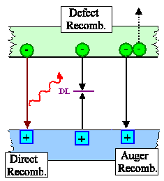
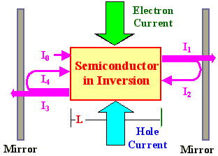
There are always several recombination channels active in parallel
|
| |||||||||||
High efficiency LED's need optimized recombination. | ||||||||||||
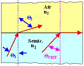
Without "tricks" only a fraction of the light produced gets out of the semiconductor |
| |||||||||||
Index grating is essential | ||||||||||||
Avoiding re-absorption is essential | ||||||||||||
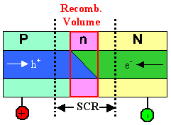
Defined recombination volumes are important | ||||||||||||
Hetero junctions of the NnP or NpP type are the solution, but create problems of their own | ||||||||||||
Hetero-interfaces must be defect free Þ Avoid misfit dislocations! | ||||||||||||
Laser diodes are similar to LED's but need to meet two additional conditions |
| |||||||||||
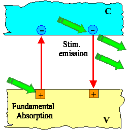
1. The rate of Stimulated emission, a new process predicted by A. Einstein concerning the interaction of light and electrons in the conduction band, must be at least as large as the rate of fundamental absorption | ||||||||||||
Stimulated emission results in two fully coherent photons for one incoming photon and thus allows optical amplification. | ||||||||||||
Strong stimulated emission his requires large non-equilibrium electron concentrations in the conduction band. Þstrong "pumping" is necessary, moving electrons up to the conduction band just as fast as they disappear by recombination. | ||||||||||||
In semiconductor junctions pumping can be "easily" achieved by very large injection currents across a forwardly biased (hetero) junction.Þ cooling problem! | ||||||||||||
2. There must be some feed-back that turns an (optical) amplifier into an oscillator for one frequency | ||||||||||||
Feed-back is achieved by partially transparent mirrors. | ||||||||||||
Monochromatic output is achieved by the optical resonator forme by two exactly plan-parallel mirrors | ||||||||||||
Only wavelengths l = 2L/i (i = integer)
that "fit" into the cavity will be able to exist. Together with the condition hn = hc/l = Eg the Laser wavelength is given |
||||||||||||
Semiconductor Lasers now span the range from IR to UV; essential materials are all III-V's, in particular the GaN family. | ||||||||||||
Molecular beam epitaxy is the deposition method of choice for epitaxial multilayer structures | ||||||||||||
|
© H. Föll (Semiconductor Technology - Script)