 |
Many if not all MEMS devices could be described as being either a sensor or an actuator |
|
 |
Accelerometers
and gyros are sensors because the
convert the non-electrical input "acceleration" or "angular velocity" into electrical signals - and
that's what sensors do. |
|
 |
The DLP Chip is an actuator because it converts electrical signals to mechanical displacements of mirrors. |
 |
It is thus a good idea to take a general look at some of the principles of sensors and actuators
incorporated in MEMS devices. Let's look at sensors first. |
|
 |
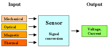
In general, we have the following simple situation: |
|
|
|
|
 |
We have all kinds of input signals - mostly but not always from the
four categories shown - and want an electrical signal as output. |
|
 |
The sensor is supposed to have two major properties.
- Maximum response to whatever is to be detected - in other words: large sensitivity
- No or very small response to all other inputs - in other words: very small cross-sensitivity
or a high selectivity.
|
|
 |
What we need to have inside the sensor is some kind of detector coupled to something that produces an electrical
signal. |
 |
Let's look at some examples to make this less abstract. We have a mechanical input - pressure,
acceleration, angular velocity, vibration, ..., whatever. |
|
 |
Inside the sensor something will respond by moving - a membrane bows according to pressure, a cantilever
bends upon acceleration, a vibrating gyro mass starts to wobble when encountering angular velocity, and so on. |
 |
Converting this movement to electrical signals
can now be done in a number of ways. |
 |
The stress or strain in the moving
part of the sensor is measured. That can be done, for example, by using the following "effects". |
| | |
| |
|
 |
Piezoresistive effect. All
materials change their resistivity if their dimensions change; with some materials (including
Si) the effect is far larger than what would be expected from geometry alone. This is called piezoresistive
effect and the reasons for this effect cannot be simply explained; you have to delve deeply into band theory for this.
| |
 |
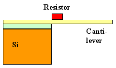
| The red material converts the deflection to an electrical output. |
|
| |
Class Exercise:
Calculate
DR/R for a rectangular piece of material with length l,
width w, thickness t and specific resistivity r
that is strained by e
in l-direction | |
|
 |
The change of the resistance if a piece of poly-Si sitting on a cantilever as shown
may be 10 - 50 times larger than what on would it expect from the geometry change alone. Measuring this change allows
to determinee and thus the deflection of the beam. |
|
|
 |
Piezoelectric effect. Some materials, alway insulators, if "squeezed"
become electrically polarized, i.e. develop a potential difference between the surfaces perpendicular to the stress direction;
details can be found in the link. |
|
|
 |
Typical piezoelectric materials are quartz (crystalline SiO2) and, most important "PZT";
short for a mixture of PbTiO3 and ZrTiO3; some details can be found in the link.
| |
|
 |
Piezoelectric materials behave like a charged capacitor with the charge depending on the strain e and thus allow to determine the deflection | |
|
 |
The word "piezo" implies that there is some connection between the two effects, but that is not
so. Materials showing large piezo-resistive effects are not piezo-electric and vice verse |
| |
|
| | |
|
 |
The deflection in the moving part of the sensor
is measured. That can be done, for example, in the following ways: | |
|
| |
| |
|
 |
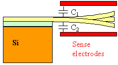
Capacitive sensing. The moving part is close to some fixed-position
electrode (on one side or on both sides). Both parts form a capacitor with a capacity C that depends on the
precise geometry and thus changes whenever the cantilever or the membrane moves. |
|
 |
| Capacitive detection of beam deflection |
|
|
 |
The movement can be "up and down" as shown in the figure or "in and out". The gyro
dealt with before contains two types of capacitive sensors as can be
easily seen: comb structures and "large" electrodes on the substrate. |
|
|
 |
Magnetic and inductive sensing is possible if one uses a ferromagnetic
material - e.g. some Ni on the cantilever. This is not a method easily implemented in Si MEMS, however. |
|
|
 |
Optical methods might be used (as in any AFM); but once more not easily in
Si MEMS technology | |
|
 |
Thermal transfer, in contrast, might be used with Si MEMS -
but not so much for detecting deflections of beams and membranes | |
| | |
| |
 |
In essence, we are left either with capacitive methods for the detection of the deflection
of some moveable part, or we use "piezo" effects. |
 |
We will not discuss the other three input case here. It is clear that we have many ways in
principle to realize the sensing of optical, magnetic, thermal or other inputs, but that the realization and optimization
of a suitable MEMS device will take a lot of R&D for every individual case. |
|  |
It is equally clear that we need special materials for this, and that progress depends to some
extent on the discovery of new effects and materials. One example for this is the discovery that Si nanowires show
a "giant" piezoresistive effect (about 40 times large than bulk Si1)) and thus might
help to increase the sensitivity of MEMS devices in years to come. |
| |
|
|
Actuators General |
| |
|
 |
Take the diagram from above and read it backwards - now you have
an actuator. Some electrical input produces an action. |
| |
| |
|
 |
Of course, the "action" might be the production of magnetic field, light, or some
heat, but usually it is a mechanical movement we want. This can be induced by producing
a force that pulls or pushes at something directly, or by just producing some pressure that acts on all surfaces the same. |
|
|
 |
Let's see what we have for that. | |
|  |
Very prominent are electrostatic
actuators. Just use your capacitor structure, apply a voltage, and there will
be forces. If we look at the structure at right, the question is, of course, what force? |
|
|
 |
Well, there is some capacity Ccomb between a finger of the comb and
a fixed plate. If we apply a potential difference U to the capacitor, some electrostatic energy EC
is stored in the capacitor given by | |
|
| | |
| |
| |
| |
| |
|
 |
This is the key equation for "capacitive forces" and you should try to derive it (in case of
doubt look at the exercise below). | |
 |
The force
FComb pulling or pushing on one element of the comb in some direction then is simply given by the
proper (negative) derivative: | |
| |
| | |
| |
| FComb | = – | U2
2 | · | dC
dy | = |
e · h· U2
x0 |
|
| |
| |
| |
 |
This calls for an exercise, of course. |
|
|
|
| |
 |
Besides using capacitors for driving some (small!) movement, thermal
actuators are in use. |
|
| | | |
|
 |
The principle, as shown in the figure, is simple and self-explaining. Thermal expansion of
a double-anchored beam will produce deflection as shown. | |
|
|
 |
Advantages are very high forces and relatively large deflections (depending on the geometry, of course). |
|
|
 |
Disadvantages are relatively high energy consumption and relatively sluggish response times. |
|
 |
With double layers ("bimetal principle") movement with just one anchor point can
be obtained, too. | |
|
 |
Thermal actuation is used for a variety of applications; most prominent, perhaps, are inkjet
systems for printers | |
| |
| | |
 |
Relatively large mechanical forces can also be produced be piezoelectric materials. For this, we use the piezoelectric sensing mentioned above
in reverse |
| | |
|
 |
The same materials as for sensing can be used, i.e. crystalline quartz or PZT, but
there are many other piezoelectric materials. | |
|
|
 |
There is a problem, however. Only materials with no inversion
symmetry can be piezoelectric, and that condition excludes all "simple" crystals. Materials with a Perowskite structure (often of the type ABO3) like
LiNiO3 are piezoelectric, but also others like ZnO or AlN. |
|
|
 |
This should give you a hint why piezoelectric drivers are difficult to implement. We have materials that
are hard to deposit. While a very thin layer that can be deposited by sputtering
in reasonable times might be good enough for sensing, the amount of force built up in a piezoelectric material is tied to
its volume, and we may need thicker layers, not easily handled by present day (2007) technology. |
|
|
 |
However, progress has been made and piezoelectric drives in MEMS may have a bright future. |
|
| |
| | |
 |
All of the above can only give a taste treat of MEMS sensors and actuators. How important the
topic is, become clear if you consider that all the computing power of microelectronics and so on comes to nought if there
is no input and no output. |
|
 |
By necessity, input and output means sensors and actuators,. Not necessarily only mechanical
output, and not necessarily MEMS devices. A flat panel display or a DLP-based beamer is an output system; the first
one without MEMS technology, the second one without it. Your keypad is an input device. Is there MEMS inside? We leave it
at that. |
© H. Föll (Semiconductor Technology - Script)
