| |
 |
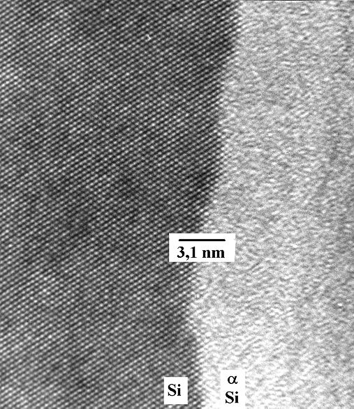
The picture below shows the boundary between crystalline Si, and Si
that has been rendered amorphous by an ion implantation (the ion beam came from the
right). The picture is slightly remarkable because it was the first high
resolution transmission electron microscopy (HRTEM) picture ever taken from damage after ion implantation. |
|
 |
There is indeed an amorphous Si (a-Si)
layer. (Think a minute how you could ascertain that without transmission electron microscopy). |
|
 |
There is a pretty abrupt, if somewhat wavy boundary between the amorphous and the crystalline
Si. |
|
 |
There seems to be little disturbance in the Si lattice - it looks pretty perfect. |
| |
|
© H. Föll (Semiconductor Technology - Script)
