 |
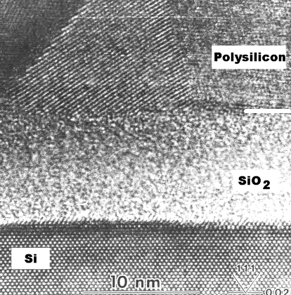
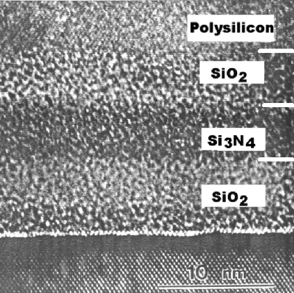
Here are two HRTEM pictures of "gate" dielectrics form around 1990 from the Siemens Laboratories
in Munich. It is actually not the gate dielectric in these pictures, but the dielectric in the capacitor
of a DRAM
memory cell. The properties of this oxide are just as critical as under the gate of a transistor. |
|  |
The one on the left show the "conventional" single layer of SiO2
that was grown by thermal oxidation. |
|
 |
The picture on the right shows "ONO". Here the first
oxide is grown by thermal oxidation of the substrate wafer, the nitride is deposited by CVD,
and the top oxide layer is produced by oxidizing the nitride. |
|
|
|
© H. Föll (Semiconductor Technology - Script)


![]() 6.2.3 CVD for Poly-Silicon, Silicon Nitride and Miscellaneous Materials
6.2.3 CVD for Poly-Silicon, Silicon Nitride and Miscellaneous Materials