 |
As far as lithography is concerned, it is evident that we need the following key
ingredients: |
|
 |
A photo
resist
1), i.e. some light sensitive material, not unlike the coating on photographic
film. |
|
 |
A mask (better known as reticle
2)) that contains the structure you want to transfer - not unlike a slide. |
|
 |
A
lithography unit that allows to project the pattern on the mask to the resist on the wafer.
Pattern No. x must be perfectly aligned to pattern No. x - 1, of course.
Since about 1990 one (or just a few) chips are exposed at one time, and than the wafer is moved and the next chip
is exposed. This step-by-step exposure is done in machines universally known as steppers. |
|
 |
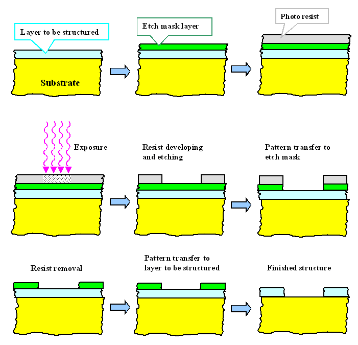
Means to develop and structure the resist. This is
usually done in such a way that the exposed areas can be removed by some etching process
(using positive resist). For some special purpose, you may also use negative resists, i.e. you remove the unexposed areas. |
 |
In principle, it is like projecting a slide on some photosensitive paper with
some special development. |
|
 |
However, we have some very special requirements. And those requirements make the whole process
very complex! |
|
 |
And with very complex I mean really
complex, super-mega-complex - even in your wildest dreams you won't even get close to imagining what it needs to do the
lithography part of a modern chip with structures size around 0,13 µm. |
 |
But relax. We are not going to delve very deep into the intricacies of lithography,
even though there are some advanced material issues involved, but only give it a cursory glance. |
| |
|
Reticles |
| |
|
 |
For any layer that needs to be structured, you need a reticle.
Since the projection on the chip usually reduces everything on the reticle fivefold, the reticle size can be about 5
times the chip size |
|
 |
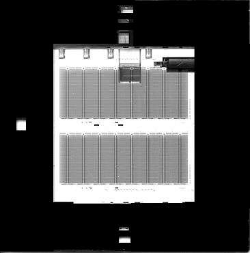
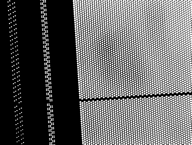
A reticle then is a glass plate with the desired structure etched into a Cr layer.
Below, a direct scan of an old reticle is shown, together with a microscope through-light image of some part. |
|
 |
"Obviously", the regular lattice of small opening in the non-transparent Cr
layer is the array for the trenches in a memory chip. The smallest structures on this reticle are about 5 µm. |
| |
 |
 |
| Typical reticle, about original size |
Enlargement (x 100) |
|
 |
Before we look at the requirements of reticles and their manufacture, lets pause
for a moment and consider how the structure on the reticle comes into being. |
| | |
|
|
|  |
First, lets look at these structure, or the lay-out
of the chip. Shown on the left is a tiny portion of a 4 Mbit DRAM. |
 |
Every color expresses one structured layer (and not all
layers of the chip are shown). |
 |
A print-out of the complete layout at this scale would easily cover a soccer field. |
 |
The thing to note is: it is not good enough to transfer
the structure on the reticle to the chip with a resolution somewhat better than the
smallest structures on the chip, it is also necessary to superimpose the various levels with an alignment
accuracy much better than the smallest structure on the chip! |
 |
And remember: We have about
20 structuring cycles and thus reticles for one chip. |
| | |
 |
The lay-out contains the function
of the chip. It established where you have transistors and capacitors, how they are connected, how much current they can carry, and so on.
|
|
 |
This is determined and done by the product
people - electrical engineers, computer scientists - no materials scientists are involved. |
|
 |
The technology, the making of the chip, determines
the performance - speed, power consumption, and so on. This is where material scientists
come into their own, together with semiconductor physicists and specialized electrical engineers (who e.g., can simulate
the behavior of an actual transistor and thus can tell the process engineers parameters like optimal doping levels etc.). |
|
 |
In other words, the reticles are the primary input of the product engineers to
chip manufacturing. But they only may contain structures that can actually be made. This is expressed in design rules which come from the production line and must be strictly adhered to. Only if all
engineers involved have some understanding of all issues relevant to chip production,
will you be able to come up with aggressive and thus competitive design rules! |
 |
What are the requirements that reticles have to meet (besides that their structures
must not contain mistakes from the layout. e.g. a forgotten connection or whatever). |
|
 |
Simple: They must be absolutely free of defects
and must remain so while used in production! Any defect on the reticle will become transferred
to every chip and more likely than not will simply kill it. |
|
 |
In other words: Not a single particle
is ever allowed on a reticle! |
 |
This sounds like an impossible request. Consider that a given reticle during its
useful production life will be put into a stepper and taken out again a few thousand times, and that every
mechanical movement tends to generate particles. |
|
 |
Lithography is full of "impossible" demands like this. Sometimes there is a simple
solution, sometimes there isn't. In this case there is: |
|
 |
First. make sure that the freshly produced reticle is defect free (you must actually check
it pixel by pixel and repair unavoidable production defects). |
|
 |
Then encase it in pellicles
3) (= fully transparent thin films) with a distance of some mm between
reticle and pellicle as shown below. |
|
|
|
|
 |
One of the bigger problems with steppers - their very small (about 1 µm) depth of focus - now turns to our advantage: Unavoidable particles fall on the pellicles and
will only be imaged as harmless faint blurs. |
 |
How do we make reticles? |
|
 |
By writing them pixel by pixel with a finely focussed electron beam into a suitable sensitive
layer , i.e. by direct writing electron-beam lithography. |
|
 |
Next, this layer is developed and the structure transferred to the Cr layer.
|
|
 |
Checking for defects, repairing these defects (using the electron beam to burn off unwanted
Cr, or to deposit some in a kind of e-beam triggered CVD process where it is missing), and encasing the reticle
in pellicles, finishes the process. |
 |
Given the very large pixel size of a reticle (roughly 1010),
this takes time - several hours just for the electron beam writing! |
|
 |
This explains immediately why we don't use electron beam writing for directly
creating structures on the chip: You have at most a few seconds to "do" one chip in the factory, and e-beam writing
just can`t deliver this kind of throughput. |
|
 |
It also gives you a vague idea why reticles don't come cheap. You have to
pay some 5000 $ - 10 000 $ for making one reticle (making the lay-out is not
included!). And you need a set of about 20 reticles for one chip. And you need lots of reticle sets during the development
phase, because you constantly want to improve the design. You simply need large
amounts of money. |
© H. Föll (Semiconductor Technology - Script)
