 |
Chemical etching is simple: Find some (liquid) chemical that dissolves the layer
to be etched, but that does not react with everything else. |
|
 |
Sometimes this works, sometimes it doesn`t. Hydrofluoric acid (HF), for
example will dissolve SiO2, but not Si - so there is an etching solution for etching SiO2
with extreme selectivity to Si. |
|
 |
The other way around does not work: Whatever dissolves Si, will always dissolve SiO2,
too. At best you may come up with an etchant that shows somewhat different etching rates, i.e. some (poor) selectivity. |
 |
Anyway, the thing to remember is: Chemical etchants, if existing, can provide
extremely good selectivity and thus meet our second request from above. |
|
 |
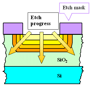
How about the first request, anisotropy? Well, as you
guessed: It is rotten, practically non-existent. A chemical etchant always dissolves the material it is in contact with,
the forming of a contact hole would look like this: |
|
|
|
 |
There is a simple and painful consequence: As soon as your feature size is about
2 µm or smaller, forget chemical structure etching. |
|
 |
Really? How about making the opening in the mask smaller, accounting for the increase in lateral
dimensions? |
|
 |
You could do that - it would work. But it would be foolish: If you can
make the opening smaller, you also want your features smaller. In real life, you put up a tremendous effort to make the
contact hole opening as small as you can, and you sure like hell don't want to increase it by the structure etching! |
 |
Does that mean that there is no chemical etching in Si microelectronics?
Far from it. There just is no chemical structure etching any more. But there are plenty
of opportunities to use chemical etches (cf. the statistics
to the 16 Mbit DRAM process). Lets list a few: |
|
 |
Etching off whole layers. Be it some sacrificial layer
after it fulfilled its purpose, the photo resist, or simply all the CVD layers or thermal oxides which are automatically
deposited on the wafer backside, too - they all must come off eventually and this is best done by wet chemistry. |
|
 |
Etching coarse structures, e.g. the opening in some protective
layers to the large Al pads which are necessary for attaching a wire to the outside world. |
|
 |
Etching off unwanted native oxide on all Si
or poly-Si layers that were exposed to air for more than about 10 min. |
|
 |
All cleaning steps may be considered to be an extreme
form of chemical etching. Etching off about 1,8 nm of native oxide might be considered cleaning, and a cleaning step
where nothing is changed at the surface, simply has no effect. |
 |
While these are not the exciting process modules, experienced process engineers
know that this is where trouble lurks. Many factories have suffered large losses because the yield was down - due to some problem with wet chemistry. |
 |
A totally new field, just making it into production for some special applications,
is electrochemical etching. A few amazing (and not yet well understood) things
can be done that way; the link provides some samples. |
© H. Föll (Semiconductor Technology - Script)
