 |
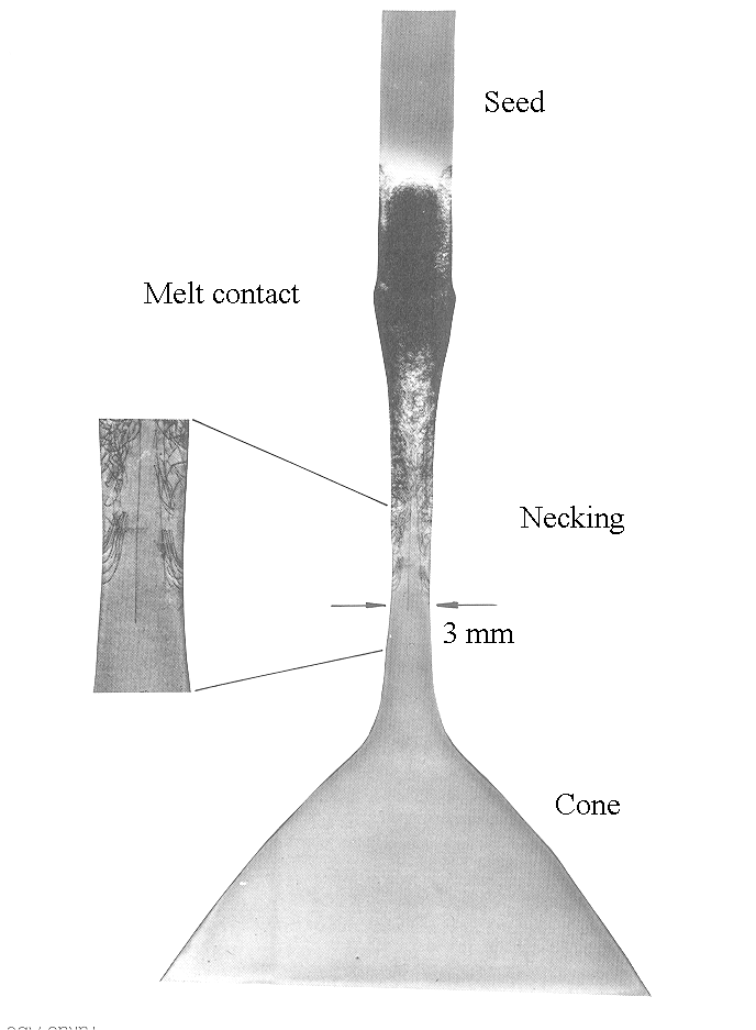
| Courtesy of Wacker / Siltronic; Burghausen, Germany |
| Here is an X-ray topograph of the first part of crystal growth | ||||
| An X-ray topograph is similar to a transmission electron microscope image - it shows the interior of the sample and dislocations are visible as dark lines. | ||||
| You see a dislocation-free seed crystal, followed by region full of dislocations. This is unavoidable because dipping a solid seed in a melt that has by definition a higher temperature, always causes a "thermal shock" with stress and strain and therefore plastic deformation. | ||||
| The the diameter of the now growing crystal is made as small as possible (it still must be able to carry the weight of the finished crystal - up to 250 kg or so). This is the "necking" or Dash process. | ||||
| The dislocations disappear after a few cm, the question is why? The picture almost shows it. For the usual <100> oriented crystal, the glide planes of the dislocations (the {111} planes) are all inclined to the growth direction, and the dislocations, still feeling some stress, will simply move out of the crystal. | ||||
| This is where the art part comes in - or better came in. Keep enough stress to move the dislocations, but not that much that new ones will be generated. | ||||
| ||||
![]() 4.1.3 Silicon Crystal Growth and Wafer Production
4.1.3 Silicon Crystal Growth and Wafer Production
![]() Czochralski Crystal Growth Process
Czochralski Crystal Growth Process
![]() The Science and Art of Si Crystal Growth
The Science and Art of Si Crystal Growth
© H. Föll (Semiconductor Technology - Script)