 |
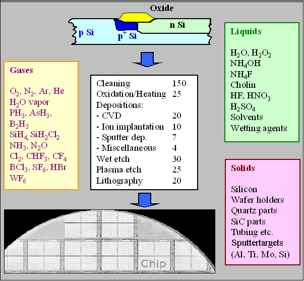
| Here is the rest of the processes | |||
| A few more materials are needed, especially solids in the form of "sputter targets". | |||
| A great total of about 450 process- and control steps are needed. | |||
| |||
| We don't have a chip yet - we only have unpackaged chips on a wafer. | ||
| Next, the wafer has to be cut and the chips that work (this needs a measurement) are packaged. | ||
| Packaging, although not needing processes at very small dimensions, is not simple either. | ||
| To continue, use the link | ||
© H. Föll (Semiconductor Technology - Script)