 |
Here are some quick questions: |
|
 |
List (and discuss briefly) some essential inputs to a chip factory. |
|  |
What is the essential process for producing raw (= metallurgical) Si and what is the
major use for this Si? |
|
 |
Go through the essential of Si single crystal growth by the CZ technique. Give
numbers and discuss in-situ doping, keeping the crystal dislocations-free, and any remaining problems. |
|  |
Describe shortly the essentials of how to obtain clean, doped poly-Si as needed for
single crystal growth |
|
 |
Where and why is a CVD process involved in making electronic grade Si? |
|
 |
Describe the phenomenon of segregation. How does it impact Si crystal growth? |
|
|
|
 |
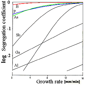
Given the diagram on the right, discuss:
- What a segregation coefficient of , e.g., 10–2 means in terms of the concentration in the crystal
in the beginning and the end of the crystal growth process if the initial concentration in the melt is 10–6
- Why you prefer As to Sb as a dopant during crystal growth .
|
|
| |
|
|
 |
Why is extreme flatness an essential condition for standard Si wafers? |
|
 |
Why is it possible to keep wafers completely free of dislocations, but not of "microdefects"
= agglomerates of point defects? |
| | |
|
© H. Föll (Semiconductor Technology - Script)
