 |
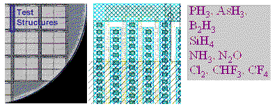
Semiconductor technology happens in factories. They need special materials, "reticles"
(= structures), "know-how" and huge amoundt of money (= capital) as major inputs |
|
|
|
 |
It's always about money! Only mass production will recover large investments. |
|
|
 |
The materials side always contains semiconductor substrates ("wafers") and often
very dangerous special "raw" materials. | |
|
 |
A number tells it all: 500 - 1.000 wafers /day are processed in a large Si "wafer
fab" | |
|
| |
| |
 |
Three big steps to Si wafers |
|
Sand (SiO2)
Metallurgical Si
Poly-Si |
Þ
Þ
Þ |
Metallurgical Si
clean (doped) poly-Si.
Single crystal / wafer |
|
|
 |
Si single crystal growth is done by "Czochralski process" (CZ). |
|
|
 |
Dislocation-free crystals are possible but "bulk microdefects" and impurities cannot
be totally avoided. | |
|
 |
Nearly perfect 300 mm wafers are standard. |
|
| |
| |
|
 |
Growing single crystals of compound semiconductors is far more difficult than
for elemental semiconductors | |
GaAs:
150 mm wafers, encapsulation technique, disl. density (103 - 106) cm–2
GaP, InP
as GaAs but smaller and more expensive
SiC:
100 mm wafers, sublimation technique, several polytypes available, "pipe" defects |
|
|
 |
Precise stoichiometry is important |
|
|
 |
Vapor pressures if the constituents at the melting point might be very different |
|
|
 |
New kinds of defects might be encountered |
|
|
 |
Polytypie might be encountered |
| |
 |
Major techniques are - Encapsulated CZ
- Sublimation growth
| |
|
| |
| |
|
| |
| |
|
| |
|
|
| |
|
| |
© H. Föll (Semiconductor Technology - Script)
