 |
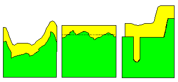
Thin films have other spatial properties besides their thickness, i.e. roughness |
|
|
|
 |
Interface roughness and surface roughness R defined by their "root mean
square". | |
|
| |
|
|
|
| R | = | æ
ç
è
| 1
N | |
N
S
i=1 | zi2 |
ö
÷
ø | ½ |
|
| |
|
| |
| |
 |
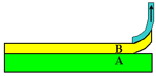
Useable thin films adhere to their substrate. |
|
|
|
 |
A direct measure of adhesion is the interfacial energy gAB
between film A and substrate B. | |
|
 |
The phase diagram provides some guideline. Complete miscibility = good adhesion, (eutectic))
decomposition =(?) low adhesion. Calculations of g are difficult. |
|
|
 |
Full adhesion can only be obtained for films grown on
a substrate. Adhesion energies can be measured. | |
| | |
| |
 |
Generally, there will be stress s and strain
e in a thin film and its substrate. |
|
Stress and strain in thin films
can be large and problematic!
|
|
|
 |
A major source of strain is the difference of the thermal expansion coefficients a | |
| | |
|
|
|
| eTF |
= |
DT · Da
| | | |
|
| sTF |
= |
Y · DT · Da |
|
| |
| |
| |
| |
 |
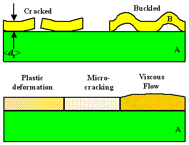
Stress in thin films may relax by many mechanisms; and this might be good or bad:
- Cracking or buckling
- Plastic deformation
- Viscous flow
- Diffusion
- Bending of the whole system (Warpage)
| |
|
|
 |
Warpage can be a serious problem in semiconductor technology. |
|
|
|
|
© H. Föll (Semiconductor Technology - Script)


