 |
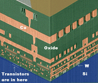
Semiconductor technology is almost synonymous with thin film technology |
|
|
|
 |
A thin film is adhering to a substrate and (at least orginally) continous. |
|
|
 |
Thin films may still be found in the product or may have been "sacrificed" during
the making of the product. | |
|
 |
An IC is a study of thin films in and on the Si substrate. |
|
|
 |
The same is true for pretty much every semiconductor product. |
|
| |
| |
| |
 |
Thin always means "thin" relative to some intrinsic (internal) length
scale. Examples are: | |
- Dimensions dx, y, z
- Grain size dgrain
- Lattice constants a0
- l radiation (light, IR, UV)
- Absorption depths
- Mean free path lengths.
- Diffusion length
|
- SCR width dSCR
- Debye length dDebye
- Critical thickness dcrit for
electrical break down
- Critical thickness dtu for
tunneling |
|
|
 |
Structural length scales | |
|
 |
Wavelength and interaction length scales |
|
|
 |
Transport parameter length scales | |
|
 |
Electrical scales | |
| | |
| |
|
 |
There are many thin film applications outside of semiconductor technolgy: |
| |
|
 |
Optical, electrical, chemical, mechanical, magnetical technologies use thin films |
| |
| | |
|
© H. Föll (Semiconductor Technology - Script)
