 |
Structure and size matter! |
|
| Typical Si wafer: |
300 mm diameter, 850 µm thick, perfect single crystal |
| Solar cell: Si |
- Single crystalline, bulk.
- Poly crystalline, large grain, bulk.
- Polycrystalline, micro grain, "thick" film
- Polycrystalline, nano grain, thin film.
- Amorphous (plus H), thin film
|
|
|
 |
Mostly we need single crystals, as perfect (and as large) as possible |
|
|
 |
Either in bulk, or thin films | |
|
 |
If thin film, substrates matter. |
|
 |
For some applications (solar cell , LCD, ...) polycrystalline or amorphous
semiconductors are used | |
|
 |
"CIGS" or CdTe for solar cells. |
|
|
 |
Amorphous or poly-Si for LCD transistor matrix |
|
| |
| |
| |
 |
Important elemental semiconductors are Si
and marginally Ge | |
| Some important Properties | Remarks |
| Lattice type, lattice constant |
Structure independent |
| Melting point, diffusion constants |
| Bandgap type and energy | | Dielectric constant |
| Thermal expansion coefficient | | Doping range |
Structure dependent |
Transport of electron / holes
(mobility, life time, diffusion length, .. |
| Unwanted levels in bandgap |
|
|
 |
Forget Se, C, P, As and b |
|
 |
Compound semiconductors are important |
|
|
 |
Group IV and compounds: SiGe, SiC |
|
| |
|
III-V compounds (Al, Ga, In) - (N, P , As, Sb). Important GaAs, GaxAl1-xAs,
GaP, InP, .. | |
| | |
Chalkogenides AxBy(S, Se, Te)2. Important "CIGS"
= CuInxGa1-xSe2 | |
| | |
"Newcomers" like organic semiconductors, Metal oxides (e.g. TiO2) |
|
 |
Properties matter! Some properties are rather independent of the structure (=
defects), others can be structure sensitive | |
| |
| |
 |
What counts in the end are products that sell and make a profit! |
|
| Integrated circuits, Solar cells, Liquid crystal displays, Micro electronic and mechanical
systems, Light emitting diodes, (Diode) Lasers, Sensors, ... |
|
|
 |
Besides the direct semiconductor products, there are also products that contain semiconductors
(PC's, Cars, TV's, any modern machine,...) and products that are needed to make semiconductor products (crystal growers,
ovens, ion implanters, ..). | |
 |
Silicon, and only
Si, enables integrated circuits of amazing complexity, with billions of transistor on one chip |
|
|
|
 |
Two kinds of integrated transistors exist.
- MOS - the absolute majority
- bipolar - if speed counts
|
|
|
 |
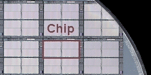
Wafers diameter are up to 300 mm (2007), smallest (lateral) structures
on a wafer are in or below the 100 nm range. | |
|
 |
Integrated circuits are packaged chips with some connections to the outside world |
|
|
| |
| |
 |
Besides integrated circuits, Si is increasingly used for other semiconductor products: |
|
|
|
 |
Solar cells based on Si consume more Si than IC's, and demand rapidly increasing Si
production. The key point of Si solar cell technology is to have high efficiencies h at
low prices. | |
|
 |
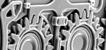
Microelectronic and micro-mechanic (and micro-optics and micro-fluidic and...) = MEMS
systems find increasing uses for many tasks. | |
| | |
| |
 |
III-V semiconducrors combine the group III elements Al, Ga, In) with the group
V elements N, P , As, Sb; giving 12 possible combinations. | |
| Properties |
Si |
GaAs |
InP |
GaP |
GaN |
In0,53Ga0,47As |
| Band gap [eV] |
1,12 | 1,42 |
1,35 | 2,26 |
3.39 | 0,75 |
| Type |
Indirect | Direct |
Direct |
Indirect |
Direct | Direct |
| Lattice |
fcc | fcc |
fcc | fcc |
hex | fcc |
|
|
 |
The most important ones are probably GaAs, InP
GaP and GaN | |
|
 |
Band gap energies and types vyr,; lattice are wurtzite or zincblende (= fcc) and sphalerite
( = hex) | |
|
| |
| |
 |
Ternary and quaternary (IIIxIII1-xVyV1-y)
compounds are relatively easy to make. | |
|
|
 |
Properties like band gap, lattice constant, refractive index then adjustable to some extent. |
|
|
 |
Main materials for optoelectronic products. Some high-speed and sensor applications. |
|
|
 |
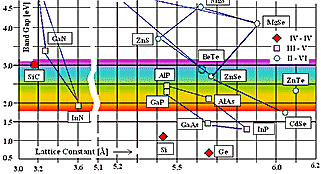
"Master diagram" = bandgap vs. lattice constant: of elementary importance for semiconductor
technology. | |
|
| |
| |
 |
Germanium (Ge) and SiC |
| |
|
 |
Germanium was almost "useless" but is experiencing some comeback now
(2007) in conjunction with Si technology. | |
|
 |
SiC is very difficult to obtain as a good single crystal (many polytypes) but has some
desirable properties for high speed or high power devices | |
 |
II-Vl
semiconductors are objects of heavy research but hardly used for products at present. |
|
|
 |
The "hot" contenders CdTe used for solar cells and actually on the market,
and, maybe ZnO in the near future. | |
|
 |
"Chalcogenides", meaning compounds with "Chalcogens", i.e.
S, Se, and Te as major elements are often semiconductors |
| |
|
 |
Oxygen, in the same IIa group, forms "oxides"! |
| |
|
 |
The most prominent representative of chalcogenides is "CIS" (CuInSe2)
or better "CIGS" (CuInxGa1-xSe2) used for solar cells and actually
on the market. | | |
 |
Organic semiconductors. A relatively recent addition to the club, organic semiconductors
seem to have a bright future in optoelectronics | |
|
|
 |
OLED's are on the market, in particular as part of a flat panel display; the first
OLED based TV screen has been announced for 2008. |
| |
|
 |
The big problem of OLED's is their sensitivity to oxygen. |
| |
| | |
|
© H. Föll (Semiconductor Technology - Script)


