| |
 |
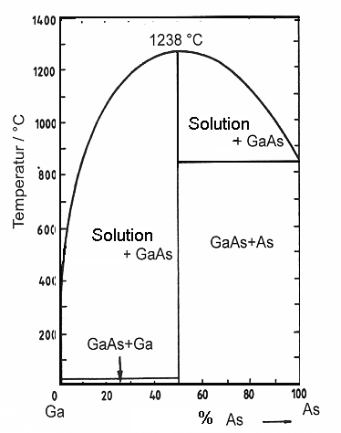
Producing GaAs crystals must starts with a consideration of its phase diagram. |
|
 |
Here it is. It is already sufficient to show that there is only a very small
region where you can get solid and stoichiometric GaAs, essentially a line. Small deviations to the left or right will produce
some liquid encasements - right after solidification and sone Ga or As related defects after complete solidification. |
| | |
|
| | |
|
| |
 |
If you think you could avoid or a least minimize those defects (that cannot possibly be good
for a device) by melting a perfect 50 : 50 mix of Ga and As, you must think again. Ga will start to evaporate out of your
mix as soon as it melts, changing the compositions. and son on..... |
 |
The message should be clear: It is far more difficult to produce a defect-free
GaAs crystal than it is possible for Si. It is actually impossible. And that is true for all compound semiconductors.
|
| |
 |
The problems with III-V technology start right here!
|
| | |
--- To be continued (or possibly not) --- |
© H. Föll (Semiconductors - Script)
