 |
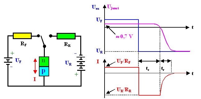
The basic situation is shown in the figure in the backbone
module which will be repeated here in a somewhat more detailed fashion. |
|
|
|
 |
We switch from a forward condition to a reverse condition at some time. The external voltage
(blue lines in the diagram) is supposed to change suddenly (we have an ideal switch) |
|  |
What we would measure in terms of the junction voltage and the junction current is shown in magenta or
red, respectively. |
|
 |
The outstanding feature is the "reverse recovery", the reverse current flowing for some time
after we switched the voltage. Right after the switching it will be limited to UR/R for
a time ts, because we can not drive more current than that through the circuit. But after ts
seconds, the current decays with some time constant tr until it reaches the small (zero in the
picture) static reverse current of the junction. |
|
 |
If we look at tr quantitatively, we take it to be the time it takes the current
to decay to 10% of the plateau value. |
|
 |
Can we calculate this behavior, which of course is the crucial behavior for the large signal switching
of a pn-junction? |
 |
Well - not without some problems. But we can understand what others have calculated. Let's
see. |
|
 |
During static forward behavior, we have a surplus of minority carriers a the edge of the space charge region,
and this surplus concentration has to disappear after we switch to reverse conditions. We looked at that in some details before, and we already have some equations for this case |
|
 |
We have to solve the relevant diffusion equation as given in the link above, but now for different conditions.
Before, we looked at the static case (i.e. ¶n min(x,t)
/ ¶t = 0, now we want to calculate how the minority carrier concentration changes
in time. |
|
 |
So, once more, we have to solve the relevant continuity equation. We do it for one side of the junction
only; the other side then is trivial. |
| |
nmin(x,t)
¶t |
= | D · |
¶2nmin(x,t )
¶x2 | – |
nmin(x,t) – n0
teff |
|
|
|
 |
The last term simply governs the disappearance of carriers by recombination; otherwise we just have Ficks
second law. For teff we have to take the minority carrier lifetime t or the transit time ttrans as the geometry demands
(in-between situations are messy!). |
 |
If we have the solution for nmin(x, t), we can calculate
everything else easily, the voltage across the junction. e.g. is
always |
| |
| Ujunct | = |
kT
q | · ln |
D nmin(x, t)
n0 |
|
|
 |
Now we have to look at the boundary conditions for the problem |
|  |
If you look at the picture above long enough, you realize that as long as Ujunct
is positive, the boundary conditions are |
| |
| IR | = |
UR
RR |
= q · D · |
¶nmin (x,t)
¶x |
|
|
|
 |
As soon as U junct = 0 V, the boundary conditions need to be changed to
|
| |
|
|
 |
You don't see it? That's OK, at least for the second case. The boundary conditions are actually only approximations,
and would take a lengthy discussion to justify them (in particular the second one and the switch over point) in detail.
So just believe it. |
 |
Now it is math - solving differential equations with certain boundary conditions. Not so easy,
but doable. According to Kingston (1953), the solutions for the two time constants ts and
tr are (in implicit form) |
| |
1
1 + IR/IF |
= | erf |
æ
ç
è |
ts
teff |
ö
÷
ø | 1/2 |
| erf |
æ
ç
è |
tr
teff |
ö
÷
ø | 1/2 |
+ |
exp –(tr/ teff
)
p ·
tr/teff | = |
1 + | 0,1 · IR
IF |
|
|
|
 |
with erf = error function as we know
it from diffusion problems. |
 |
OK. May the force be with you when you try to prove these solutions or just to extract data.
Only one thing is clear: We better look at the ratios
ts/teff and
tr/teff than at the t 's directly. |
|
 |
Well, there are always the approximations, which we are going to use here: |
| |
|
 |
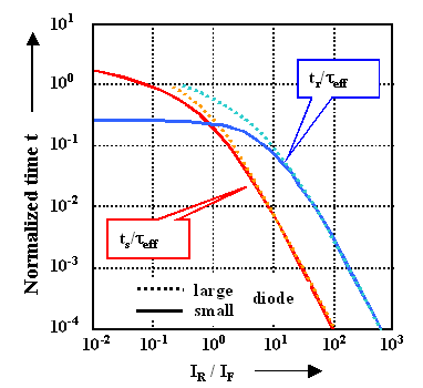
Even better, there are complete solutions in graphical form: |
| | |
|
|
|
| | |
|  |
The solid lines are for the "small" diode, where we have to take the transit time for teff, the dashed line indicate the "large" diode case. |
 |
It is clear that you really can achieve much larger switching speeds for a given teff
by being smart about I
R/IF, i.e. if you increase IR (or decrease IF,
but that is rarely an option) |
|
 |
However, don`t forget the prize you have to pay: Large reverse currents while "idling" = large
losses = heating your device. |
 |
This is the first inkling we get that there is some trade off between
speed and power. |
| | |
© H. Föll (Semiconductors - Script)

