Strain engineering involves straining of the silicon crystal to increase the mobility of charge carriers in the channel (electrons in NMOSFETs and holes in PMOSFETs). An added benefit is that it reduces the source/drain series resistance. Compressive strain is induced in PMOS transistors, typically using epitaxially grown SiGe source/drain and/or a compressively strained nitride layer over the gate. The greatest emphasis is given to the PMOSFET, since hole mobility is typically three orders of magnitude less than electron mobility. In NMOS transistors, a tensile strained nitride layer is used. These processes induce approaches that have proven to be the most manufacturable and cost-effective, and were first implemented in manufacturing at the 90 nm node.
Warum? Weil Si, das unter (erheblicher) eleastischer Spannung steht, höhere Beweglichkeiten (= mobility) zeigt.
Sowohl kompressive Spannungen /Dehnungen als auch Zugspannungen/ Dehnungen ("Tensile") werden verwendet.
Since electrons move faster through silicon with a (100) orientation and holes move faster through silicon with a (110) orientation (the orientation of most substrates), hybrid orientation technology (HOT) has developed to increase drive current as well. This approach, so far pursued mainly by IBM (East Fishkill, N.Y.), has resulted in 20% reduction in gate delays on bulk silicon. Though this process may be limited by complexity and cost, engineers are working on simplifying the process and making it more manufacturable.
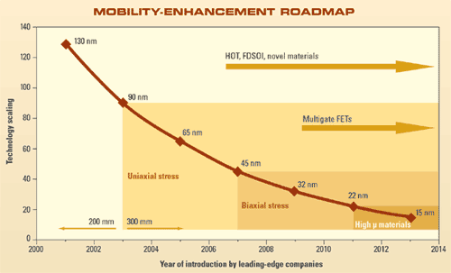
Another method that can be used is biaxial strain or global strain, where the entire wafer is strained by various methods. This approach is not likely to enter manufacturing until the 32 nm node or later because of defectivity and integration issues (Fig. 2). However, it is expected to complement process-induced (primarily uniaxial) approaches at some point.
 |
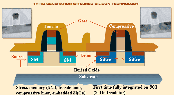
| Fig. 1. Four stress techniques — dual stress liners, stress memorization (SM) and an embedded SiGe S/D — were fully integrated on a partially depleted SOI substrate. (Source: IBM and AMD) |
As mentioned previously, AMD, together with IBM and Toshiba (Tokyo), developed a third-generation strained silicon technology that combined dual stress liners, stress memorization in the NMOS, and embedded SiGe in the PMOS devices.1 Figure 1 shows an illustration of the cross-sections of the devices with SEMs. The device was manufactured on partially depleted SOI using a 90 nm process and scaled to a 65 nm process. A novel integration scheme was used to embed SiGe very close to the gate. SiGe growth is prior to transistor implants. Tensile strain is memorized into the NMOS using poly implants and a stress transfer film that is annealed and removed. After nickel silicidation, the compressive liner was deposited and removed from the NMOS region; then the tensile liner was deposited and removed from the PMOS region. The researchers noted that resistance and poor surface mobility can significantly limit drive current improvements for a given stress-induced mobility improvement. Resistance must be reduced through NiSi process optimization, and attention to layout interactions is important between compressive and tensile liners, which exert biaxial stress.1 PMOS and NMOS saturation drive current increased by 53% and 32%, respectively, leading to 40% higher product speed. Resistance reductions were imperative to gaining the full additive benefits of the stressors. Novel methods will be needed in the future to accommodate stress-induced mobility increases. Next-generation SiGe stress methods will employ higher germanium content and tighter spacing between the gate and S/D regions.
In another combination of dual stress liners and embedded SiGe, researchers from Toshiba and Sony (San Jose) explored the scalability of these approaches.4 They used simulation to examine stress in X and Y dimensions for dense transistor layouts. In these cases, channel stress in the X direction increases to its peak right before the space between the electrodes is filled; then it declines rapidly. Stress in the Y direction increases as thickness increases, even after the space is filled. Therefore, the optimal stress configuration is when the stress liner almost completely fills the space between dense transistors. Between device generations, if gate length is constant, channel strain decreases as gate spacing decreases. Stress decreases because the total volume of SiGe decreases as gate space decreases. However, both X and Y stresses stay the same with scaling because recess depth, sidewall and gate-height scaling compensate for the lack of gate-length scaling. For the 32 and 22 nm nodes, Toshiba and Sony modeled necessary stress levels assuming 70% scaling per generation. Generally, liner stress needs to be improved by 11% and 35% for the 32 and 22 nm nodes, respectively, to maintain performance.
The mobility roadmap in Figure 2 indicates that HOT, fully depleted SOI, novel materials and multigate FETs may be combined with uniaxial stress methods, as well as biaxial stress methods, as early as the 45 nm generation. However, it will be only the most cost-effective techniques that will be used, especially for low-power applications.
Man muss das hier aber noch nicht verstehen!
 |
| Fig. 2. Mobility roadmap. At or beyond the 45 nm node, hybrid orientation technology and biaxial stress (global stress) are likely to join already implemented stress liners and embedded SiGe layers for strain engineering. To date, these technologies have been shown to be additive. (Source: R. Jammy, IBM/Sematech) |
Die "nm" geben die Dimensionen der dann zu machenden kleinsten Strukturen an.
Spannend ist der "uniaxial" und "Biaxial stress".
Noch spannender sind die "High µ materials", d.h. Materialien mit höheren Beweglichkeit als Si. Man wird sie brauchen, kennt sie aber noch nicht.