 |
Lets just look at a list of requirements for resists. We
need to have: |
|
 |
High sensitivity to the wavelength used for
imaging, but not for all optical wave lengths (you neither want to work in the dark, nor expose the resist during optical
alignment of the reticle which might be done with light at some other wave length). Not easy to achieve for the short wave
lengths employed today. |
|
 |
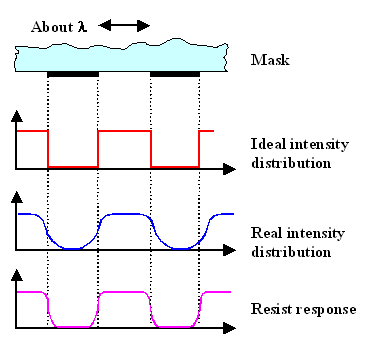
High contrast, i.e. little response (= "blackening")
to intensities below some level, and strong response to large intensities. This is needed to sharpen edges since diffraction
effects do not allow sharp intensity variations at dimensions around the wavelength of the light as illustrated below. |
| |
|
|
 |
Compatibility with general semiconductor requirements
(easy to deposit, to structure, to etch off; no elements involved with the potential to contaminate
Si as e.g. heavy metals or alkali metals (this includes the developer), no particle production, and so on). |
|
 |
Homogeneous "blackening" with depth - this means
little absorption. Simply imagine that the resist is strongly absorbing, which would mean only its top part becomes exposed.
Removal of the "blackened" and developed resist than would not even open a complete hole to the layer below. |
|
 |
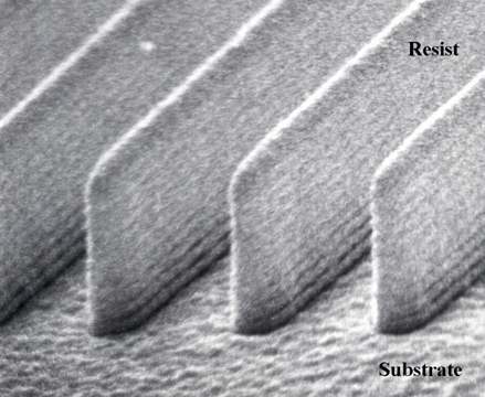
No reflection of light, especially at the interface resist
- substrate. Otherwise we encounter all kinds of interference effects between the light going down and the one coming up
(known as "Newton fringes"). Given the highly monochromatic and coherent nature
of the light used for lithography, it is fairly easy to even produce standing light
waves in the resist layer as shown below. While the ripple structure clearly visible in the resist is not so detrimental
in this example, very bad things can happen if the substrate below the resist is not perfectly flat. |
| |
|
|
 |
This would call for a strongly absorbing resist - in direct
contradiction to the requirement stated above. Alternatively, an anti-reflection coating
(ARC)
might be used between substrate and resist, adding process complexity and cost. |
|
 |
Suitablity of the resist as direct
mask for ion-implantation or for plasma etching. |
|
 |
Easy stripping of the resist, even after it was turned
into a tough polymer or carbonized by high-energy ion bombardment. Try to remove the polymer that formed in your oven from
some harmless organic stuff like plum cake after it was carbonized by some mild heat treatment without damaging the substrate,
and you know what this means. |
 |
Enough requirements to occupy large numbers of highly qualified people in resist
development! |
|
 |
Simply accept that resist technology will account for the last 0,2 µm or so in
minimum structure size. And if you do not have the state-of-the-art in resist technology, you will be a year or two behind
the competition - which means you are loosing large amounts of money! |
| |
|
|
Stepper |
| |
|
 |
A stepper is a kind of fancy slide projector. It projects the "picture"
on the reticle onto the resist-coated wafer. But in contrast to a normal slide projector, it does not enlarge
the picture, but demagnifies it - exactly fivefold in most cases. Simple in principle,
however: |
 |
1. We need the ultimate in optical resolution! |
|
 |
As everybody knows, the resolution limit of optical
instruments is equal to about the wave-length l. More precisely and quantitatively we have
|
| |
|
|
 |
With dmin = minimal distinguishable feature size;
i.e the distance between two Al lines, and NA = numerical aperture of the optical system
(the NA for a single lens is roughly the quotient of diameter / focal length; i.e. a crude measure of the
size of the lens). |
|
 |
Blue light has a wave length of about 0.4 µm, and the numerical apertures NA
of very good lenses are principally < 1; a value of 0.6
is was about the best you can do (consider that all distortions and aberrations troubling optical lenses
become more severe with increasing NA). This would give us a minimum feature size of |
| |
|
|
 |
Since nowadays you can buy chips with minimum features of 0.18 µm or even 0.13
µm; we obviously must do better than to use just the visible part of the spectrum. |
 |
2. Resolution is not everything, we need some depth of focus, too. Our substrate is not perfectly flat; there is some topography (not to mention that the Si wafer is also not perfectly flat). |
|
 |
As anyone familiar with a camera knows, your depth of focus
Df
decreases, if you increase the aperture diameter,
i.e. if you increase the NA of the lens. In formulas we have |
| |
| Df |
» |
l
(NA)2 |
= | 0.4
0.62 |
= 1.11 µm |
|
|
|
 |
Tough! What you gain in resolution with larger numerical apertures, you loose (quadratically)
in focus depth. And if you decrease the wavelength to gain resolution, you loose focus depth, too! |
 |
3. We need to align one exposure exactly on top of the preceding one. In other words, we need a wafer stage that
can move the wafer around with a precision of lets say 1/5 of dmin - corresponding to 0.18/5
µm = 0.036 µm = 36 nm. |
|
 |
And somehow you have to control the stage movement; i.e. you must measure where you are with
respect to some alignment marks on the chip with the same kind of precision. We need
some alignment module in the stepper. |
|
 |
Alignment is done optically, too, as an integral (and supremely important) part of stepper
technology. We will, however, not delve into details. |
 |
4. We need to do it fast, reliable and reproducible - 10 000 and more exposures
a day in one stepper. |
|
 |
Time is money! You can't afford more than a few
seconds exposure time per chip. |
|
 |
And you also can not afford that the machine breaks down frequently, or needs frequent alignments.
Therefore you will put your stepper into separate temperature and humidity controlled enclosures, because the constancy
oft these parameters in the cleanroom (DT » 1 oC)
is not good enough. You also would need to keep the atmospheric pressure constant, but ingenious engineers provided mechanism
in the lens which compensates for pressure variations of a few mbar; still, when you order a stepper, you specify
your altitude and average atmospheric pressure). |
 |
How do we built a stepper? By combining elements from the very edge of technology
in a big machine that costs around 10.000.000.000 $ and that can only be produced by a few specialized companies. |
|
 |
The picture below gives an impression. The basic imaging lens of the stepper is
a huge assembly of many lenses; about 1 m in length and 300 kg in weight. |
| |
|
| |
|
 |
We need intense monochromatic light with a short wave length. If you use colored light, there
is no way to overcome the chromatic aberrations inherent in all lenses and your resolution will suffer. |
 |
The wave lengths employed started with the so-called g-line (436 nm) of Hg,
fairly intense in a Hg high pressure arc lamp and in the deep blue of the spectrum. It was good down to about 0.4
µm as shown in the example above. |
 |
Next (around 1990) came the 365 nm
i-line in the near ultra violet (UV).
This took us down to about 0.3 µm. |
 |
Next came a problem. There simply is no "light bulb"
that emits enough intensity at wavelengths considerably smaller than 365 nm. The (very expensive) solution were so-called
excimer Lasers, first at 248 nm (called deep UV lithography), and eventually
(sort of around right now (2001)), at 194 nm and 157 nm. |
| |
| | |
|
 |
Next comes the end. At least
of "conventional" stepper technology employing lenses: There simply is no
material with a sizeable index of refraction at wavelengths considerably below 157 nm that can be turned into
a high-quality lens. Presently, lots of people worry about using single
crystals of CaF2 for making lenses for the 157 nm stepper generation. |
 |
What do you do then? First you raise obscenely large
amounts of money, and than you work on alternatives, most notably |
|
 |
Electron-beam lithography. We encountered
it before; the only problem is to make it much, much faster.
As it appears today (Aug. 2001), this is not possible. |
|
 |
Ion beam lithography. Whatever it is,
nobody now would bet much money on it. |
|
 |
X-ray lithography. Large-scale efforts
to use X-rays for lithography were already started in the eighties of the 20 century (involving huge electron
synchrotons as a kind of light bulb for intense X-rays), but it appears that it is pretty dead by now. |
|
 |
Extreme UV lithograpy at a wave length
around 10 nm. This is actually soft X-ray technology, but the word "X-ray lithography" is
loaded with negative emotions by now and thus avoided. Since we have no lenses, we use mirrors. Sounds simple - but have
you ever heard of mirrors for X-rays? Wonder why not? This is what the US and the major US companies favor at present. |
 |
Well, lets stop here. Some more advanced
information can be found in the link. |
|
 |
But note: There are quite involved materials
issues encountered in lithography in general, and in making advanced steppers in particular. CaF2 is an
electronic material! And the success - or failure - of the global enterprise to push minimum feature size of chips beyond
the 100 nm level, will most likely influence your professional life in a profound matter.
|
|
 |
This is so because the eventual break
down of Moores law will influence in a major
way everything that is even remotely tied to technology. And what will happen is quite
simply a question if we (including you) succeed in moving lithography across the 100 nm barrier. |
| |
|
© H. Föll (Electronic Materials - Script)

