| Here is an article from the Semiconductor International from February 2002 | |
| At a Glance | ||
| Calcium fluoride will likely remain the lens material of choice for 157 nm lithography tool designs, engineers having come up with various tricks to offset birefringence problems. But optics and system developers have their work cut out for them. | ||
157 nm Optics Demand a Bag of Tricks
Calcium fluoride. That material has evoked a roller coaster of hopes and fears in a chipmaking industry gearing up for 157 nm lithography and the finer features that it enables. Lithographers have for years relied on readily available fused silica for system lenses, but the material does not transmit well at 157 nm. Enter CaF2, identified as a possible savior to 157 nm technology.
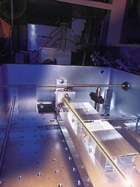
However, the difficulties that come with crystalline materials caused concern that the industry would not be able to get the quantity or quality it needed. But engineers persevered, producing generations of CaF2 and overcoming various technical barriers, such as distortion and stress-induced birefringence. Various organizations were working together to help CaF2 suppliers improve their growth processes. Things were looking up. (For a discussion of preliminary life-test results of CaF2 [Fig. 1], see "Testing Optical Damage for 157 nm Lithography".)
 |
| Fig. 1 Testing the life time of CaF2 |
By July, at International SEMATECH's workshop on CaF2 birefringence, the situation was apparently under control. There was relief as researchers showed compensation techniques that could be used to minimize the impact of birefringence. CaF2 birefringence wasn't going to be a big problem after all.
Today, technologists are surging ahead with optical techniques, aiming to have 157 nm research tools available by 2003 and production tools by 2005. At the same time, though, they are perhaps more realistic about the formidable challenges that lie ahead. Yes, they have come up with a bag of tricks to compensate for the intrinsic birefringence of CaF2, but those tricks are going to prove difficult and costly, both in terms of time and money.
Although it took the industry by surprise initially, lithographers are relieved that birefringence will not be the showstopper once thought, said Stephane Dana, product manager at ASML (Veldhoven, Netherlands), in charge of 157 nm lithography. Since then, ASML has been taking measurements, along with lens supplier Carl Zeiss (Oberkochen, Germany), and they have become more confident. "We will be able to compensate for it in the optical design," Dana said. "We know we can solve it. The problem is that it puts even more pressure on CaF2."
Countermeasures will require more effort, time and money, noted Phil Ware, senior fellow, lithography, at Canon U.S.A. Inc. (Irving, Texas). "However, the impact on Canon's 157 nm tool schedule is relatively minor. We expect about a half-year delay for the beta tool (from the first half to the second half of 2003), mainly due to the additional time it will take to grow CaF2 crystals with different orientations."
Refraining from refractiveLithography system manufacturers plan to put at least part of their faith in catadioptric designs, combining lenses and mirrors in an optical system to minimize chromatic aberrations. Whereas previous optical systems have been primarily refractive designs, replacing some lenses with mirrors helps to minimize the use of CaF2 . All toolmakers will have to rely on various forms of catadioptric systems, Dana noted. Alternatives — such as line-narrowed lasers and practical alternative crystal materials — have not progressed enough to allow continued use of refractive designs, he said. However, Dana declined to give details of ASML's catadioptric design (for the most part, toolmakers are holding that information close to their chests).
Some proposed approaches have featured multiple axes with beam splitters or mirrors, Ware noted. "Canon's approach uses a concentric off-axis catadioptric design with only two mirrors," he said. "This design not only uses fewer elements, but it lends itself to the same kinds of assembly and tuning techniques that we have optimized for our all-refractive optics."
Besides minimizing the use of CaF2, optical designers must now consider the orientation of the CaF2 crystals in their designs. Lithographers have been using lenses made with crystal orientations of [111]. Although clocking these crystals around the optical axis has been suggested as a way to mitigate the birefringence problem, it's not enough. Designs will have to combine [111] crystals with CaF2 crystals of other orientations to solve the problem more effectively.

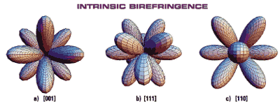
2. These 3-D models show the directional dependencies of CaF2 ’s intrinsic birefringence. (Source: NIST)
"At this point the designers have stated in the conferences that they will pursue the strategy of catadioptric designs using [001], [111] and possibly [110] clocked pairs, and combining them so that the residuals partially cancel," Burnett said.
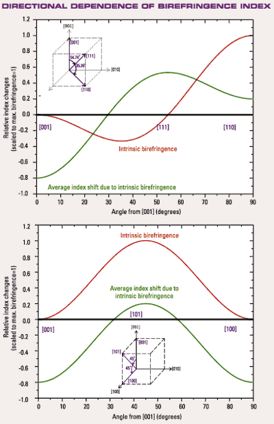
The orientation of the lenses is an important factor because intrinsic birefringence depends on the direction in which light propagates through the CaF2, which is a function of the cubic crystal direction (Fig. 2). For [111] lenses, birefringence is zero as long as the light doesn't stray from the central direction of the lens. Unfortunately, the angle dependence of this model (Fig. 3) doesn't bode well for lenses with high numerical aperture (NA), which are essential for achieving the resolution necessary for smaller feature sizes. Lenses made with [001] crystals, which are less affected by rays outside the central angle, will particularly help to minimize birefringence, Burnett said.

3. Quantitative values (scaled to 1 at the maximum) demonstrate the directional dependence of intrinsic birefringence
as well as the resulting index anisotropy. (Source: NIST)
Canon's design incorporates a combination of [110], [100] and [111] crystal orientations to reduce aberrations, Ware said. ASML plans to clock elements of [111] and [100] oriented CaF2, Dana said. Nikon's primary approach will also be a catadioptric design, combining crystal orientations and clocking strategies, noted Chris Sparkes, director of technology at Nikon Precision (Belmont, Calif.).
Another factor that must be considered, Burnett said, is that the angle dependence of the effect results in an anisotropy of the average index on the scale of the birefringence effect. "This effect also results in wavefront errors and must be considered in the design for minimizing the distortion." The effect has a different angle dependence and different impact on the optical performance, he noted, "so it must be treated separately using the various optical compensation methods."
Since presenting its findings to the industry, NIST has confirmed by measurement the full angle dependence of intrinsic birefringence predicted by the original model, Burnett said, and the model is generally accepted as correct. Optical Research Associates (ORA, Pasadena, Calif.) has incorporated the model into its widely used CODE V lens design software. CODE V can now account for the effects of intrinsic birefringence approximately.
To add to the difficulties, clocking the lenses to compensate for birefringence limits the freedom to clock the lenses to compensate for surface figure and index aberrations, Burnett noted. "This aberration clocking has always been required to build projection lens systems for longer wavelengths," he said. "Restricting this aberration clocking freedom (e.g., to 120° for [111] lenses) because of correcting for intrinsic birefringence may require tighter surface figure and index specifications."
Quality and quantityPutting all the additional requirements together only makes matters worse for the supply and availability of high-quality CaF2. The quantities available have been an ongoing concern because most CaF2 suppliers are still on a fairly steep learning curve. CaF2 is used in conjunction with high-purity fluoride crystals for 193 nm lithography, and has already faced a shortage of materials, noted Gitimoy Kar, director of the Fluoride Crystals Business at Corning Inc. (Corning, N.Y.). Growing sufficiently large crystals is a difficult process, he said.
Now materials suppliers must not only meet increasingly stringent specifications for [111] CaF2, but they must grow high-quality crystals in other orientations as well. "Crystal growth is a very slow process; it takes months to grow one ingot," Kar said. "Then you have to multiply the cycle time by the number of orientations you have to grow it in."
Corning acquired the capability to produce CaF2 in 1999, and has since quadrupled its manufacturing capacity. Other CaF2 suppliers have worked to expand capacity as well. For example, Schott Lithotec AG (Mainz, Germany) announced last year a third production plant for CaF2 monocrystals. A subsidiary of Schott Glas, Schott Lithotec was established in 1998, launching its second crystal production facility in 1999.
In an effort to maintain some control over CaF2 supply, toolmakers are also producing some of their own. Last summer, Nikon Precision noted ramp-up of its own CaF2 production. Although it would not constitute the majority of its supply, it would be significant in helping the company get the quality it needed. Canon Inc.'s wholly owned subsidiary Optron Inc. (Yuuki City, Japan) inaugurated its CaF2 crystal manufacturing facility in August, with Canon then claiming itself as the world's largest CaF2 manufacturer. "When it reaches full capacity over the next year or so, it should meet all of Canon's CaF2 needs and then some," Ware said. For now, Canon continues to buy crystal materials from multiple outside sources, he noted.
With all the capacity expansions, it seems as if the industry ought to have CaF2 coming out its ears. Unfortunately, all the capacity in the world doesn't resolve the fact that yields are reportedly in the single digits. Suppliers keep specific yield numbers to themselves — and there is certainly some discrepancy as to what specifications are considered in any yield quote — but yield is "very low," Corning's Kar conceded.
It doesn't help that toolmakers keep tightening specifications and adding measurement requirements, he said. "The industry needs more standardization for crystal specifications," he said. "We spend an enormous amount of time just characterizing materials." But there is certainly room for improvement and progress is being made. ASML's Dana said that the industry needs to see a yield increase of about 25% to get the quantities needed.
"In absence of high yield, people are putting in more furnaces, which is very capital-intensive," Kar said. Although the investment may be worthwhile, it is difficult to continue pouring money into materials for 157 nm lithography when 193 nm lithography has not been generating sufficient revenues. "The industry is in a recession," Kar said. "With all the effort we had put into 193 nm applications, we still need to generate revenues. At the same time, we're being asked to accelerate RD for 157."
Although crystal growers are primarily relying on the standard Bridgman-Stockbarger method, startup Single Crystal Technologies (SCT, Gilbert, Ariz.) has a crystal growth technique that could increase yields to some 90%, according to Kiril A. Pandelisev, CEO and chief science officer (see Semiconductor International, December 2001). Pandelisev contends that improving purification and yield levels is the key to dealing with birefringence issues (see "CaF2 Birefringence, Purity and 157 nm Technology").
Mixing it inAnother option in the battle against intrinsic birefringence is the possibility of combining CaF2 with other crystal materials. Having shown that CaF2 has birefringence values that are opposite those of BaF2 and SrF2, NIST researchers believe alternate materials may prove useful in compensating for the effect.
"Our main effort now in this area is exploring the possibility of creating mixed crystals," Burnett said, noting examples of CaxBa(1-x)F2 and CaxSr(1-x)F2. "With appropriate values of x (Ca content) determined from our measured values, these should have no intrinsic birefringence at 157 nm, if high-quality materials can be made."
Several CaF2 suppliers are working with NIST on this project, according to Burnett. "This approach is appealing since it could eliminate the problem completely," he said. "Such mixed crystals have been successfully grown before for certain ranges of component ratios. However, it remains to be seen whether the other properties such as absorption, index homogeneity, and stress-induced birefringence can be maintained within specifications. Also, given the aggressive 157 nm schedule, the industry cannot count on it, at least for first-generation tools."
Toolmakers seem to be shying away from this approach for compensation, at least for the time being, because alternate crystal materials do not offer the necessary properties. "We really don't see the quality that we need, and certainly not in the quantity we need," Dana said. "So ASML is not considering this as an option."
Canon and Nikon do not currently plan to use either BaF2 or SrF2 for 157 nm tools either. "CaF2 has introduced its own set of challenges, even after considerable experience in lithography tools," Nikon's Sparkes said. "The use of BaF2 is even less mature and presents even greater challenges."
The materials are not practical for lens fabrication, Canon's Ware agreed. "Barium fluoride still does not meet the transmission requirements at 157 nm," he said. "It also has 100× greater water solubility than calcium fluoride. This phenomenon would require development of new surface treatment technologies (for instance, we have to use water for lens polishing). ... Based on the information presented to date, we doubt that anyone will successfully use these kinds of materials for full-field 157 nm production lenses."
Whatever the solutions — or, more precisely, whatever the final combination of solutions — may be, it is clear that researchers have their work cut out for them. Intrinsic birefringence certainly complicates system designs and fabrication. Although any hopes of keeping 157 nm lithography on schedule are perhaps a bit optimistic, the semiconductor industry is no stranger to the challenge.
| For more information... | ||
| When you contact any of the following manufacturers directly, please let them know you read
about them in Semiconductor International. | ||
| ASML |
Canon |
Carl Zeiss
|
| Corning |
Cymer |
Nikon Precision |
| NIST |
Schott Lithotec
|
Single Crystal Technologies |
|
![]() Some Issues from Advanced Lithography
Some Issues from Advanced Lithography
© H. Föll (Electronic Materials - Script)