 |
Silicondioxide (SiO2) has been the "ideal" dielectric
with many uses in chip manufacture | |
- Gate oxide for Transistors
- Dielectric in Capacitors
- Insulation
- Stress relieve layer
- Masking layer
- Screen oxide during Implantation
- Passivation
|
|
|
 |
Only recently (2007) is it replaced by "low k"
and "high k" dielectrics, i.e. dielectrics with a dielectric constant either lower or larger
than that of SiO2 | |
|
 |
"Low k" dielectrics (polymers, porous SiO2, ..; the ideal
material has not yet been found) are used for intermetal insulation; low k is important here to keep the RC
time constants small | |
|
 |
"High k" dielectrics (the present front runner is HfO2)
will replace the gate oxides. They can be somewhat thicker than SiO2 without sacrificing capacity, while
strongly reducing tunneling currents. | |
| | |
|
 |
SiO2 can be made in several ways: |
|
- Dry thermal oxidation:
- Wet thermal oxidation:
- "Chemical Vapor Deposition"
(next sub-chapter)
- "Spin-on techniques
(next sub-chapter)
- "Anodic oxidation (presently not
used in technology) |
|
|
 |
Dry oxidation is relatively slow but gives best oxide qualities as defined by:
- Uniformity
- thickness control
- Break down field strangt
- Interface quality
- Reliability
Typical use: Highest quality gate oxid. |
|
|
 |
Wet oxidation is about 10 times faster; it is used whenever relatively thick oxides are needed.
Typical use: Field oxide. | |
|
 |
The other methods are needed whenever there is no Si available for oxidation (e.g.
intermetal dielectrics). | |
| | |
| |
|
 |
As long as the process is diffusion controlled (i.e. the time it takes oxygen
to diffuse through the already formed oxide determines rates, the thickness increases protorional to t1/2 |
| |
|
 |
For thin oxides the growth rate is reaction controlled and the thickness - time dependence
becomes complicated. | |
| | |
| |
 |
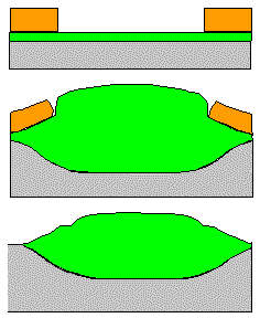
Growing oxide only locally ("LOCOS") was a key process for field oxides. |
|
|
|
 |
Without a "buffer" oxide below the masking nitride, large mechanical strain develops,
producing plastic deformation and thus dislocations around the oxide edges. |
|
|
 |
These "Oxide edge dislocations" kill the transistor. |
|
|
 |
Buffer oxides solve the problem, but create new problems: A "birds beak" develops,
increasing lateral dimensions beyond the mask dimension. | |
 |
"LOCOS" is a good example for a universal feature of Si technology:
Solutions to "old" problems create new problems. Solutions to the new problems... and so on. It follows:
- Process complexity increases all the time.
- New materials are needed all the time.
|
|
|
|
|
© H. Föll (Electronic Materials - Script)
