 |
Advanced devices nowadays use a box isolation technique. However, the accepted name for that
is "shallow trench isolation" or STI. |
|  |
If the trench is "deep" you may still call it
STI, or possibly DTI, but this abbreviation may also mean "double trench isolation"
- just get used to the fact that the semicoductor industry moves to fast to have time for standardizing those things and
to force people to stick to it. |
 |
How is it done? And why do we need it? Let's just look at this issue very briefly. |
 |
First, we note that all the problems with LOCOS already mentioned in the backbone get rapidly worse as dimensions get smaller. On top of that, new problems develop,
and the process flow becomes increasingly complicated (and expensive). |
|
 |
Many problems would disappear if you just would etch a suitable "hole", i.e. a trench in your
substrate wherever you need isolation, and then fill it with oxide. |
|
 |
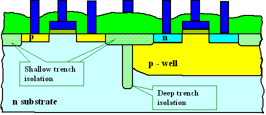
Or CMOS structure from before then
would look like this: |
| |
|
|
 |
Of course, nobody would superimpose a shallow and a deep trench isolation as shown (you just would have
the deep one and move the transistors closer together), but the picture illustrates the point nicely. |
|  |
So why wan't it done long since? |
 |
Because it is neither easy to etch the required trenches, to fill them with (high-quality)
oxide, and to planarize the surface. |
|
 |
The latter point is the key: Whatever process you use to fill the trenches
with oxide, after your oxide deposition you have oxide everwhere, and you must take it off again wherever you don't want
it, i.e. outside the trenches |
|
 |
If you wonder why you fill the trenches with oxide, and why you don't
use simple thermal oxidation anymore, you missed some the essentials! Figure it out
yourself; it is enough to consider what would happen if you start thermally oxidizing your Si after you etched the
deep trench. |
| | | |
© H. Föll (Electronic Materials - Script)
