 |
If you run a cathode, emitting
an electron beam, with large electrical fields between the cathode and the anode, you
will find that your workfunction
EA seems to change to smaller values as the field strength increases. |
|
 |
This is called Schottky
effect; it is observed at large field values of (105 - 108)V/cm.
|
 |
If you apply even higher field strengths (and remember: E = U/d; you do
not need high voltages U, only small dimensions d), EA seems to vanish
altogether. |
| |
|
|
|
|
 |
This effect is is called field emission. It works even
at room temperature and is barely temperature dependent, so it can not be a temperature activated process. |
| |
 |
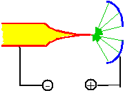
Field emission is rather easy to obtain: all you have to do, is to make a very fine tip with
a curvature of the tip in the nm - range as shown on the left. |
| |
 |
Field emission might then occur with a few Volts between the anode and the tip, because all
the field lines will have to converge on the small tip. |
|
|
 |
How can we understand these effects? Whereas the Schottky effect
is relatively straight forward, field emission is a manifestation of the tunnelling
effect, a purely quantum mechanical phenomenon. |
 |
Lets look at how the free electron gas model
must be modified at high field strengths - and we will be able to account for both effects. |
|
 |
The potential energy E outside of the material is such that electrons
are to be extracted - it is not constant, but varies with the field strength E simply as
|
| |
|
|
 |
E, the (constant) applied field strength (written in mauve to make sure that we do not mix it up with the energy
E). We have the following situation: |
|
|
|
|
 |
Simply summing up the energies graphically yields the qualitative energy curve for an electron
at the edge of a crystal as shown below. |
|
|
|
|
 |
Whichever way you superimpose the potential energies, the potential barrier to the outside
world will always be reduced. This explains qualitatively the Schottky effect. |
 |
The field emission effect requires a somewhat
different consideration. |
|
 |
Lets look at the extremes of the Schottky effect. For
really high field strengths the potential barrier gets even lower and thinner, it may look somewhat like this: |
| |
|
 |
Now the tunneling effect may occur. It is
a phenomenon inherent in quantum mechanics and allows electron "waves" to "tunnel"
through a potential barrier. |
|
 |
In other words, the value of the wave function
y
for an electron does not got to zero abruptly at a potential barrier, but decays exponentially. There is then a finite amplitude
for y
on the other side of the potential barrier, an effect that is felt if the barrier is
"thin" and low - as in the picture above. If the field strength is high enough, large quantities of electrons
can directly tunnel to the outside world. More about tunnelling in the link. |
 |
Field emission thus is a purely quantum mechanical effect; there is no classical
counterpart whatsoever. It is used in a growing number of applications: |
|
 |
Electron microscopes for special purposes (e.g.
scanning electron microscopes with high resolution at low beam voltage, a must for the chip industry) are usually equipped
with field emission "guns". |
|
 |
"Scanning Tunnelling Microscopes"
(STM)
which are used to view surfaces with atomic resolution, directly employ tunnelling effects. |
|
 |
Large efforts are being made to construct flat panel displays with millions of miniature field
emission cathodes - at least one per pixel. |
|
 |
Some semiconductor devices (e.g. the "tunnel diode")
depend on tunnelling effects through space charge regions. |
 |
In other contexts, tunnelling is not useful, but may
limit what you can do. Most notorious, perhaps, is the effect that very thin
insulators - say 5 nm and below - are insulating no more, a growing problem for the chip industry. |
|
|
| |
|
© H. Föll (Electronic Materials - Script)
