 |
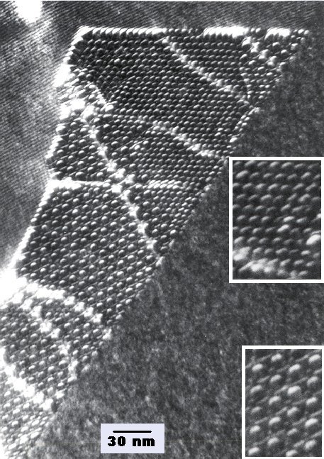
Here is the picture of a small angle twist grain boundary once
more at a larger size. The transition from one kind of network to the other kind is not prominent in the micrograph;
the prominent white lines are extrinsic dislocation accommodated in the network. |
 |
The topic in this module is not something you have to know for an examination, or for being
considered knowledgable about defects. It just illustrates two general points about grain boundaries: |
|
 |
Even relatively simple situations can become very complicated (for us, not for the crystal). |
|
 |
Seeing a boundary in the electron microscope, and understanding what you see, is not the same
thing. |
| |
|
 |
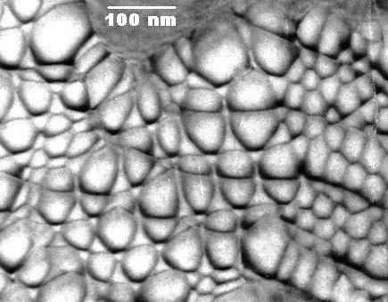
Below is essentially the same situation showing the same kind of small angle twist boundary,
but imaged with some special kind of bright field condition that gives good resolution and shows all dislocations at the
same time. The changes in the network can be seen somewhat more clearly; the twinned region is on the right hand side. |
| |
|
|
 |
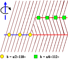
In a cross-section, the whole structure looks like this: |
| | |
| |
|
 |
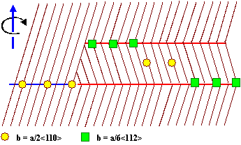
The traces of some {111} lattice plane across the twist boundary are shown; neglecting the (small) twist for sake of clarity.
|
 |
The boundary may split into two twin boundaries with a superimposed
network of the proper DSC lattice dislocation (shown as green squares) |
| | |
|
 |
This picture, however, gives rise to a question: Where is the network of a/6<112>
dislocations? In the "upper" or "lower" twin boundary? Could it also be in between as a regular network
of a/2<110> dislocations split into partials? |
|
| |
|
|
| |
 |
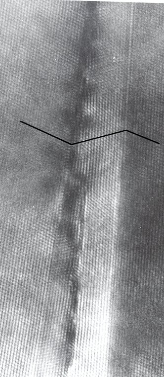
This picture gives the answer. It shows a HRTEM cross-section of an artificially made small angle
grain boundary in Si. It contains a large tilt component and probably some twist. |
| | |
 |
The dislocations can be seen, partially as ending lattice planes, partially by a general localized disturbance
of the picture (darkish areas). |
| |
|
 |
They obviously change form the perfect crystal (S = 1 case) to one of
the twin boundaries (S = 3 case). In the S = 1 case
we would see the network with the extended and constricted stacking fault nodes, in the S
= 3 case we would see a regular hexagonal network of a/6<112> dislocations. |
| | |
 |
We thus may have to expect all the possibilities shown below: |
| | |
| |
| | | |
|
|
| | |
| |
| |
|
 |
This means, among other things: |
|
 |
If we see a dislocations network clearly belonging to a S = 1
case, it does not mean that the grain boundary is not split into twins. Possibly, this may even be true for a S
= x boundary, which may be split into two boundaries with S = y
and S = u with a suitable relation between y and u. |
|
 |
It is not easy to understand why the crystal does this. For our case we might surmise that
the energy gain by having low energy a/6<112> dislocations in a S = 3 interface
is about equal to the energy needed to create the two twin boundaries since both possibilities occur without much preference
between the two. |
| |
|
© H. Föll (Defects - Script)
![]() 7.2.3 Case Studies: Small Angle Grain Boundaries in Silicon II
7.2.3 Case Studies: Small Angle Grain Boundaries in Silicon II ![]() Dislocation Network in a Si - NiSi2 Interface
Dislocation Network in a Si - NiSi2 Interface