 |
 |
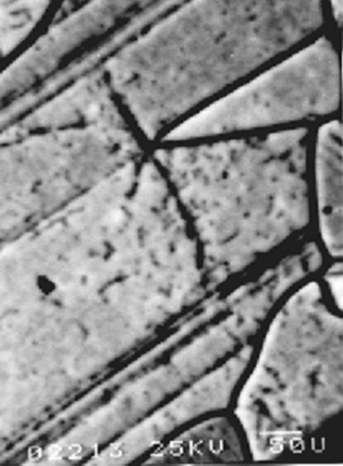
active defects in solar-grade Si.
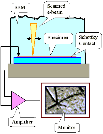
| The "Electron Beam Induced Current method (EBIC) employs a (SEM) on a sample with a thin electron-transparent Schottky contact (usually evaporated Al). The Schottky contact is biased in reverse, the leakage current is amplified and displayed on a monitor synchronized with the electron beam scan. | |||||
| The elecon beam induces carriers; the minority carriers either recombine at defects or are collected at the Schottky contact as current with the resulting signal being displayed on the monitor. | |||||
| The picture on the monitor thus shows the efffective minority carrier life time. Defects that are "electronically active" reduce the currents; they appear in dark contrasts. | |||||
|
| ||||
| Principle of EBIC | Typical EBIC picture, showing electronically active defects in solar-grade Si. |
||||
![]() 6.1.1 Observation of Dislocations and Other Defects
6.1.1 Observation of Dislocations and Other Defects
![]() < Comparison of Anodic Etching to Chemical Etching and EBIC
< Comparison of Anodic Etching to Chemical Etching and EBIC
© H. Föll (Defects - Script)