 |
The differential etch rate during anodic etching depends on the current density.
At small current densities, defects may etch much faster than perfect Silicon; anodic etching than reveals the defects very
clearly. |
| |
|
 |
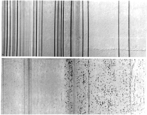
Shown are adjacent areas of a Si specimen that was grown for solar cell
applications. It contains many grain boundaries, preferably twin boundaries, and dislocations. |
|
 |
The upper pictures was obtained after etching with a rather large current density. Only grain boundaries
can be seen; but this may be due to steps between different grains
because the etching rate depends on the grain orientation. |
|
 |
The lower picture shows the area etched with low current densities. Many grain boundaries are no longer
visible (despite the fact that we know they must be there), but a large number of dislocation etch pits is visible. |
 |
Comparing anodic etching with chemical etching gives a similar result: |
|
|
 |
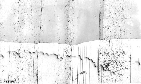
The upper half of this sample was anodically etched, the lower with a purely chemical
etch (Secco-etch
in this case). |
|
 |
Evidently the anodic etch does not show some grain boundaries. From
other experiments it became clear that anodic etching under these condition shows only electronically
active defects, i.e. defects that influence electronic properties, especially the carrier life time. |
| |
© H. Föll (Defects - Script)


![]() 6.1.1 Observation of Dislocations and Other Defects
6.1.1 Observation of Dislocations and Other Defects