 |
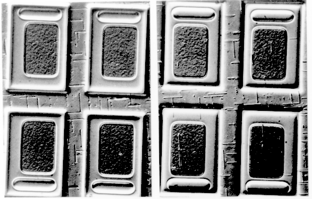
Stacking faults revealed by the so-called "Secco etch" for 30 seconds in transistors. For
one kind of process we can see different phases of the stacking fault generation by process-induced "forces" by
looking at wafers from different stages of the process: |
|
|
|
 |
Here we see bipolar transistors where just the collector contact (the oval part)
and the base region (the rectangular part) have been defined. We have: |
|
 |
Small stacking faults only outside the transistor areas (the rectangles) on the left-hand side |
|
 |
Large stacking faults inside and outside the transistors on the right-hand side. These
stacking faults may actually be rather complicated structures akin to
the one shown in the backbone text. |
|
|
|
 |
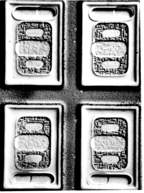
Now we have progressed to the emitter (the two smaller ovals) the base contact
(the bigger oval) and the highly doped contact area of the collector (the small oval in the bigger collector contact oval) |
|
 |
We have small stacking faults in high density only in the base region (including the contact). The others
either vanished (unlikely) or were not produced in this wafer. |
|
 |
What that looks like at high magnifications as seen
by transmission electron microscopy can be seen in the link. |
 |
The question is: Will the transistors work? The answer is: It depends. |
|
 |
The transistors without any stacking faults will work, but their leakage currents may still be considerably
higher than the leakage currents in transistors without any stacking faults in the neighborhood. |
|
 |
The transistor with large stacking faults in their interior will most likely not work at all. They will
have a short-circuited emitter-base diode. |
|
 |
The transistors with small stacking faults will mostly work, (albeit not too well), but some of them will
be dead. The likelihood of "death by stacking fault" increases with the stacking fault density. This puzzle could be solved by TEM. |
 |
We also can see that the alignment of the structures to the <110>
direction of the wafer is rather poor (the rectangles are not parallel to the traces of the stacking faults) and the alignment
of the structures is not too good either (the base contact, e.g., is not at the exact center of the base). |
| |
© H. Föll (Defects - Script)


![]() 6.1.1 Observation of Dislocations and Other Defects
6.1.1 Observation of Dislocations and Other Defects ![]() Oxidation Induced Stacking Faults in Silicon
Oxidation Induced Stacking Faults in Silicon