 |
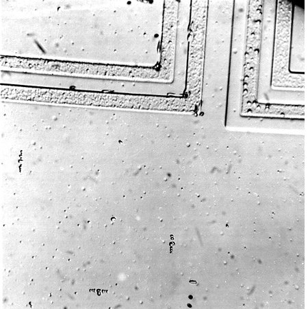
Shown is a preferentially etched part of an integrated circuit. Many kinds of
defects are revealed; the interpretation is not necesarily clear. |
|
 |
The big etch pits in the frames of device parts are due to dislocations. |
|
 |
In the structureless area we see pits and hillocks (distinguished because the "black-white vector",
the vector from the black part of a small contrast to the white part comes with both signs) and a few very distinctive features
consisting of a central pit with "satellites" along one direction. |
| |
|
|
 |
All these features are most likely due to precipitates. The rows of pits are caused by precipitates that
produced a sequence of dislocation loops to relieve the stress in a process known as "prismatic
punching". |
 |
What prismatic punching looks like
if imaged with a transmission electron microscope at high magnfication can be seen in the link |
| |
© H. Föll (Defects - Script)

![]() 6.1.1 Observation of Dislocations and Other Defects
6.1.1 Observation of Dislocations and Other Defects