Pictures to: 4. IBM T.J. Watson Research Center


4.1 TEM of Silicon - Silicide Interfaces    Publication 25

What follows are the pictures to publication 25 (Cross-sectional TEM of silicon-silicide interfaces).
One of the pictures (FIg. 2 in the paper) shows the very first high-resolution image of a heterogeneousa interface.
     
 
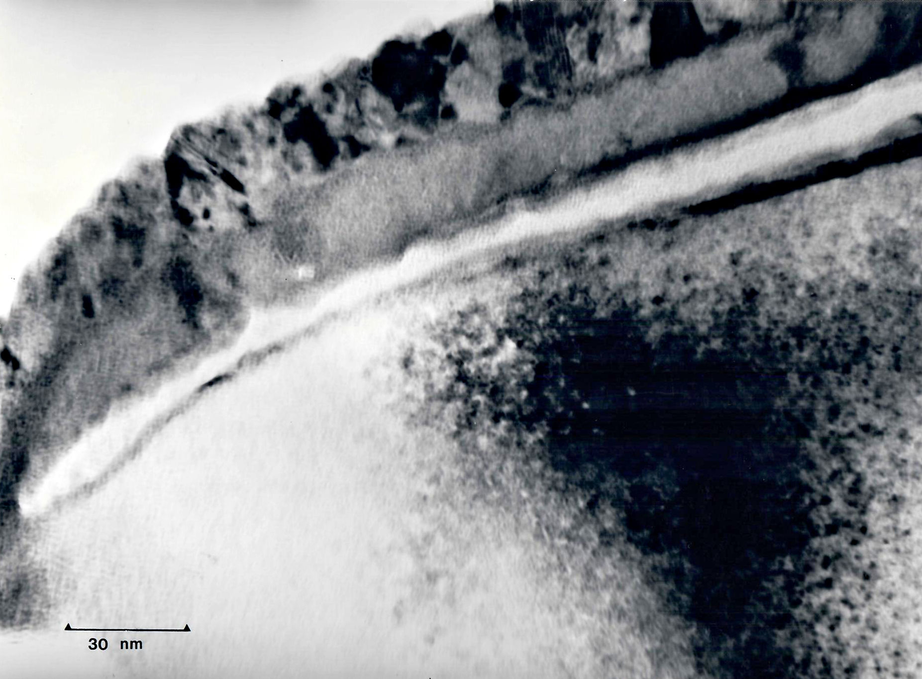
TEM silicid esi inteface; Pd2Si
Fig. 1 In Publication 1
What you see going from th from bottom of the picture to the to top: Si; nothing (because of denomination), Pd2Si (structuress since very likely epitaxial to the Si)
and unreacted Pd The picture demonstrates the problems of cross-sectional TEM with heterogeneous samples.
Many reasons for stress lead to bending and in thise case even to delamination of the Pd2Si / Pd layer from the Si substrate.
FIG. 1. Thin layer of Pd2 Si and Pd on Si. The layer is severely bent (comingout of the paper plane in the left-hand corner).
 
HRTEM silicid esi inteface; Pd2Si
Fig. 2 In Publication 1. Epitaxial Pd2Si (top) on Si (bottom)
My most treasured picture. It is the very first HRTEM of a heterogeneous interface ever taken. Wasn’t easy then.
Fig. 2. Lattice image of the Pd2 Si-Si interface. The spacing oft he Si {111}fnnges . (e.g. parallel to the interface) is 0.31 nm. A Burgers-like circuit isdrawn in, showmg 79 Pd2 Si {22-40} fringes for 75 Si {111} fringes
 
HRTEM silicid esi inteface; Pd2Si
Auxiliary picture to Fig. 2 In Publication 1
Showing that ther eis morre than one picture and a "large" pseudo Burgers circuit.
The "cut" resukts from glueing two pictrues together.
 
HRTEM silicid esi inteface; Pd2Si
Auxiliary picture to Fig. 2 In Publication 1
Just for showing details. The bright spot on the lower right is simply light emitted by the hot cathode
way up in there in the microscope column. You only get that way down on the screen fior a perfectly aligned microscope.
 
TEM silicid esi inteface; NiSi2
Fig. 3 In Publication 1.
FIG. 3. Heavily faceted NiSi2 2 on {100} Si. Parts of the silicide have beenremoved during ion milling; the surface of the silicide therefore is not theoriginal silicide surface.
 
HRTEM silicid esi inteface; Ni2Si2
Fig. 4 In Publication 1
Another "first" as far as HRTEM of heterogeneous interfaces are concerned
 
TEM silicid esi inteface; NiSi2
Fig. 5 In Publication 1.
FIG. 5. Misfit dislocations in the Si-NiSi {100J} interface and dislocationsin the silicide.  
 
TEM silicid esi inteface; NiSi2
Fig. 6 In Publication 1
FIG. 6. Misfit dislocations in the Ni-NiSi2 interface viewed flat-on. A hex-agonal network (lower right-hand corner; one set of dislocations not incontrast). a square network (Ieft-hand corner; one set of dislocations not incontrast), and one irregular rectangular network can be seen.
 
TEM silicid esi inteface; NiSi2
Fig. 7 In Publication 1.
 
HRTEM silicid esi inteface; NiSi2
Fig. 8 In Publication 1.
A picture that proves my original point: Even in the author's print of the journal article you can't see anything in Fig. 8
Forghget copies and scans.
FIG. 8. Lattice image of the Si-NiSi2 interface on a {111} plane. The NiSi2 istwinned with respect to the Si matrix; this also can be seen from the typicaltwin-diffraction pattern. The interface contains a dislocation at tthe darkspot.
 
TEM silicid esi inteface; NiSi2
Fig. 9 In Publication 1.
FIG. 9. Misfit dislocations in the interface between NiSi2 and {1111} Si.
 
TEM silicid esi inteface; NiSi2
Similr to Fig. 10
FIG. 10. Flat-on view of misfit dislocations in the Si-NiSi2 {111} interface.The micrograpb was taken with multibeam ditfraction conditions close tothe {111} pole
 
TEM silicid esi inteface; NiSi2
Auxiliary to Fig. 10 In Publication 1.
Once more the remacable dislocations structure in the direct and twinned epitaxial growth of the NiSi2on Si.
 
TEM silicid esi inteface; PtSi
Fig. 11 in Publication 1.
The PtSi layer is not transparetn to the electron beam at this picture.
It does show the interface geometry and the existence opd stress at the protrusion in the inteface.
FIG. 11. Interface between Si and PtSi (two sampies wirb the silicide sideglued together).

With frame With frame as PDF

go to 1. Introduction, 1.1 .Why Oh Why? 1.1.1. What it is all about

go to

© H. Föll (Archive H. Föll)