Requirements for Chip Metallization

The metal lines connecting transistors or other components on a Si chip must meet many, partially conflicting, requirements. Below is a list, including some materials that do not meet the particular requirement very well.
Can you guess the winner?
Desired Property Materials not meeting requirement
Very good conductivity All but Ag, Cu
High eutectic temperature with Si
(> 800 oC would be good)
Au, Pd, Al, Mg
Low diffusivity in Si Cu, Ni, Li
Low oxidation rate; stable oxide Refr. Metals, Mg, Fe, Cu, Ag
High melting point Al, Mg, Cu
Minimal interaction with Si substrate Pt, Pd, Rh, V, Ni , Mo, Cr (form silicides easily)
Minimal interaction with poly Si Same as above
No interaction with SiO2 Hf, Zr, Ti, Ta, Nb, V. Mg, Al
But must stick well to SiO2 ?
Must also comply with other substrates, e.g. TiN ? (see example for Al below)
Chemical stability, especially in HF environments Fe, Co, Ni, Cu, Mg, Al
Easy structuring Pt, Pd, Ni, Co, Au
Electromigration resistant Al, Cu
.... and many more,...

The winner is: Aluminum (with <1% of Si and Cu added).
Al, in fact, is pretty bad - but all others are worse!
Presently (2001) a switch to Cu takes place (the better conductivity is definitely needed). The industry will pay several 109 Dollars to develop the new material technology and change the production facilities.
 

Al Grain Structure on Different Substrates

Around the late eighties, the necessity came up to use a diffusion barrier between the Al - metallization and the Si substrate becasue the rection of Al with the Si in contact holes with cross sections < 1 µm2 became a problem. One material of choice was TiN, another one Ta.
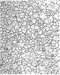
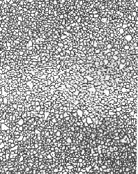
The grain structure of the Al layer (and with it other properties, e.g. the electromigration resistance, depends significantly on the substrate).
Below you can see the representative pictures (identical scale) that illustrate this point.
Al on Ta
Aluminium layer on top of a Ta layer
Al on TiN
Aluminium layer on top of a TiN layer
Close examination revealed that the substrate influences:
  1. Grain size.
  2. Grain size distribution.
  3. Texture.
  4. Degree of Si precipitation.
  5. Macroscopic stress.
  6. Microscopic stress.
All of these properteis may influence the performance ot the Al conductor - and this gives you an idea of what it means to introduce a new material into a fine-tuned product.
 

With frame With frame as PDF

go to 6.3.1 Physical Processes for Layer Deposition

go to 6.2.3 CVD for Poly-Silicon, Silicon Nitride and Miscellaneous Materials

go to Doping Trench walls

© H. Föll (Semiconductor Technology - Script)