 |
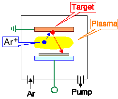
Sputter deposition |
|
|
|
 |
Plasma technique Þ Vacuum + high voltage
(and possible high frequency): complicated and expensive | |
|
 |
Layers amorphous to highly defective Þ needs usually
annealing after deposition. | |
|
 |
Very versatile because of easy control of layer composition by target composition |
|
|
 |
Decent depositioen rates possible. Particularly suited to conductors. |
|
|
 |
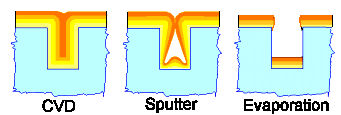
Coverage is not conformal! |
|
|
| |
| |
 |
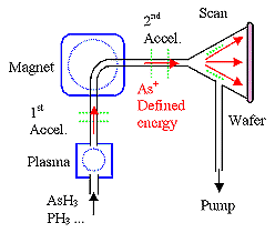
Ion implantation |
|
|
|
 |
Depth (< ca. 1 µm) and dose precisely controllable. |
|
|
 |
Very compley and expensive | |
|
 |
Method od choice for making doped layers. |
|
|
 |
Introduces defects or destroys crystallinity Þ annealing
at high T (> 800 oC) is a must | |
| | |
| |
|
 |
There are many more techniques for producing thin layers |
|
 | | Comparing edge coverage |
|
|
 |
Evaporation. Relatively simple but limited as to materials and edgencoverage |
|
|
 |
Molecular beam epitaxy. (MBE) Standard for III-V's |
|
|
 |
Spin-on techniques ("Sol- Gel"). Used for making photo resist layers; occasionally
for others | |
|
 |
Galvanics. Kind of crude but necessary for Cu interconnects in modern IC's |
|
 |
| Edge coverage may be the decisive property! |
|
|
|
|
© H. Föll (Semiconductor Technology - Script)


