 |
Let's do an extremely simple experiment that produces a "thin film" with quite mysterious
properties: |
|
 |
We take a piece of Si and immerse it into some electrolyte that can only react with
the Si by forming SiO2; acetic acid or (diluted) HNO3 or whatever, will be fine
in principle. |
|
 |
Now we take a big power supply (a "galvanostat") and run a constant (anodic) current
through the Si - electrolyte interface. The necessary chemical reaction occurring is the formation of SiO2
- nothing else is possible. |
|
 |
So we start to build up a thin layer of SiO2 on top of the Si substrate.
But SiO2 is an insulator, so it will impede current flow. Our power supply must keep the current constant,
so it will crank up the voltage as the SiO2 layer gets thicker. Eventually, the voltage will go to infinity....
? |
 |
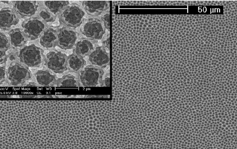
Interestingly, this is not what happens. The voltage will
go up in the first few minutes or so, but then it will stay more or less constant. The thickness of the SiO2
layer formed, will also stay more or less constant. Moreover, it will, on occasion, form interesting self-organized structures
as shown below. Now we have a puzzle! |
 |
First we have to realize that the SiO2 layer will be under tremendous compressive
stress. Why, you might ask. The temperature, after all, is room temperature and constant throughout the experiment. |
|
 |
Well, when a certain volume of Si is oxidized, you essentially put an oxygen atom in
between two Si atoms. In consequence, if you oxidize 1 cm3 of Si, you get almost 2 cm3
of oxide. Since the oxide film being formed cannot expand in lateral directions, and is perfectly brittle at room temperature,
a very large compressive stress builds up rather quickly. At a thickness of about 12 nm it is so large that something
must happen; the thickness just can't go up very much anymore. |
|
 |
On the other hand, as long as a constant current flows through the interface, we are producing
oxide at a constant rate. The thickness thus should increase linearly with time. |
 |
"Obviously", we must have a mechanism that allows to get rid of oxide at the same
rate it is being formed so the thickness can stay halfway constant. |
|
 |
Any suggestions? The best, researchers could come up with so far is that the oxide "cracks off"
somehow. But nobody really knows how that is supposed to happen. |
|
|

"Thin" layer of anodically formed oxide on Si. Not the self-organized pattern and the "grainy"
structure of the oxide |

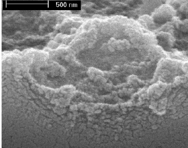
Cross-section through on "dimple. The interface between the Si and the SiO2 is not visible;
it is somewhere at the bottom of the picture. Note the "microcracks" |
S. Frey, B. Grésillion, F. Ozanam, J.-N. Chazalviel, J. Carstensen,
H. Föll, and R.B. Wehrspohn,
"Self-Organized Macrostructures in anodically formed mesoporous silica",
Electrochem. Sol. State Lett. 8(9), B25 (2005). |
|
© H. Föll (Semiconductor Technology - Script)

