 |
Imagine a piece of perfect single crystalline Si that you have turned into
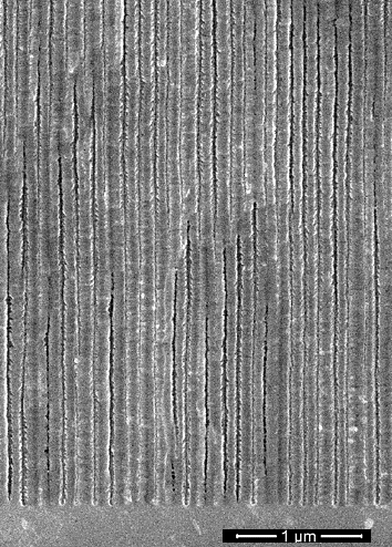
a sponge by drilling holes into it that meander around like, well, just like in a sponge. |
|
 |
Now imagine that the diameter of your holes is only a few nm, and that the average
distance between the holes is also just a few nm. Now ask yourself: Where is my periodic potential that I need in
order to evolve a band structure? How many atoms do I need to be lined up in some periodic arrangement before I can talk
about a periodic potential? Two are probably not enough, but 200 might do. |
|
 |
Tricky question. Let's simplify this a bit by considering a quantum
wire - a Si crystal arbitrarily long but with a very small diameter. As long as the diameter is a few 10
nm, nothing happens. You have a nice semiconductor, just a bit on the small side. Now decrease - in your mind - the
diameter to just a few nm. You will now encounter "quantum wire" effects.
With decreasing diameter the bandgap (perpendicular to the wire length) seems to increase and finally you just get a bunch
of discrete energy levels - because you are loosing your periodic potential. |
|
 |
Now look back at your sponge. Between the pore, you have some quantum wire like pieces of
Si. You must expect that the Si sponge behaves different from solid Si. |
 |
As it turned out in 1991, a Si sponge on a nm scale is extremely
easy to make - all you need is a simple electrochemical cell with Si as the anode through which you run some current
at the right conditions. |
|
 |
Your Si sponge actually falls into a new class of materials called "metamaterials";
man-made things with properties not encountered in the constituents. For reasons deeply routed in ancient chemistry, all
materials with pores in the size range below 10 nm must be called microporous
and not nanoporous (s would be proper).by sone codifies convention. I know it makes
not sense, but it comes from chemistry, for God's sake.. |
|
 |
The properties of microporous Si are just amazing. To give just two:
- It behaves like a direct semiconductor with a band gap of 1.5 eV or so (depends on porosity), showing strong
luminescence.
- If you put oxygen-rich stuff in the pores (e.g. KCLO4) you have produced a high explosive with three
times the bang (as measured in kJ/kg) than TNT
|
 |
Beside microporous Si, we have also mesoporous (10 nm - 50 nm) and
macroporous (> 50 nm) Si; many other semiconductors can also be turned porous. |
|
 |
Porous semiconductors are objects of active research. Many possible uses have been proposed,
none is on the market right now. |
|
 |
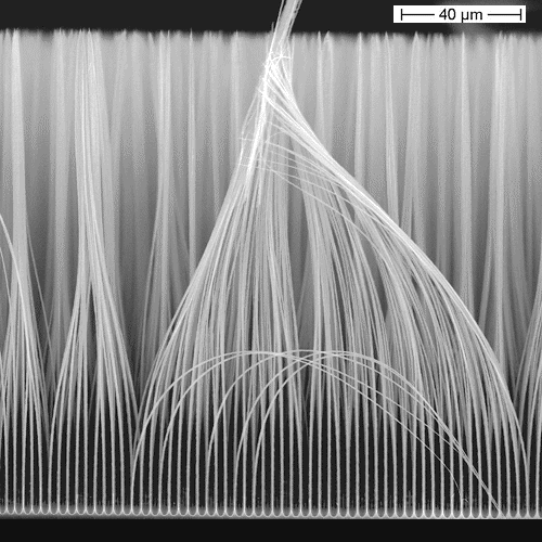
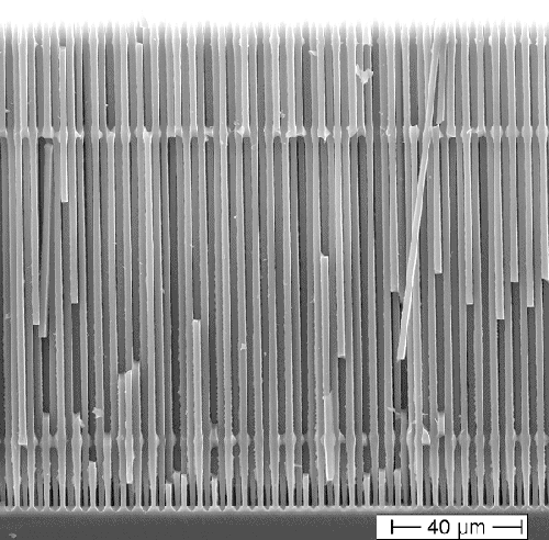
The picture below shows Si nanowires (actually
microrwires but nowadays we call all that "nano" because it's more sexy); they were made via pore etching. The
structure has been optimized for an extremely hot new application: Anodes in Li
ion batteries with an 11-fold capacity increase relative to the state-of-the-art. If you want to know more, use
the link. |
| |
 |
 |
| Si "nanowires" made via electrochemical pore etching. |
|
© H. Föll (Semiconductor Technology - Script)
