 |
If we take a transistor (bipolar or MOS), a light emitting device made
form GaAlAs, GaP, whatever, a Laser diode, a simple rectifying diode (pn-junction or Schottky junction),
i.e. just about any device made from semiconductors, we may modulate any of its input parameters (either a little bit or
a lot), and see what happens to all other parameters. The paradigmatic experiments, of course are |
|
 |
MOS transistors: Modulate the gate
voltage, see what the source-drain current does. |
|
 |
Bipolar transistors: Modulate the base current, see what
the emitter-collector current does. |
|
 |
Rectifying diodes: Modulate the terminal voltage, see
what the device current does. |
|
 |
Solar cell: Modulate the light flux, see what the photo
current or the photo voltage does. |
|
 |
Light emitting diodes: Modulate the injection current, see what the light output does |
|
 |
Laser diodes: Modulate the pumping (i.e. the injection
current), see what the light output does. |
|
 |
The list could be expanded, and many variants are possible. |
 |
Generally, we have highly non-linear systems and a simple sinus modulation of
the input parameter In in the form of |
|
|
| In(t ) = In0 + Inm ·
sin (w · t) |
|
|
|
 |
Or, expressed more generally using complex notation |
| |
| In(t) = In0 + Inm · exp
(i · w · t) |
|
|
|
 |
This simple input function, however, in general, will
produce responses that are no longer sinus shaped, but contain higher harmonics. |
 |
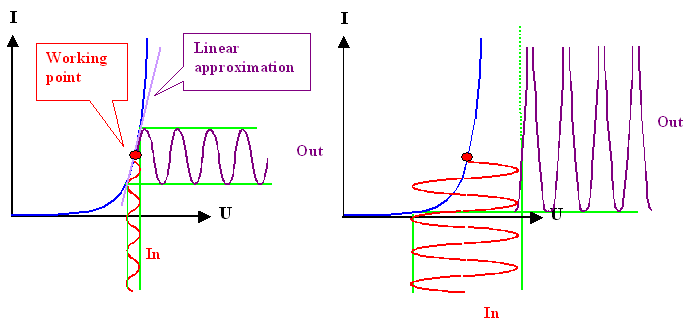
It is thus useful to distinguish between two basic modes
of frequency responses, illustrated below for a simple rectifying diode. |
|
 |
As long as the input modulation is kept small,
the response will be linear. This is called the small signal response or behavior.
|
|
 |
Large modulations or signals then obviously give the (non-linear) large
signal response. |
| |
|
|
 |
Shown is the small signal response on the left, and the large signal response on the right.
Note that the reponse in any case is directly given by the shape of the I-U characteristic and thus is not directly dependent on the frequency. |
|
 |
That, however, must be an oversimplification. At high frequencies we must
expect deviations from the 1:1 correspondence of input and output via the characteristics, and it this behavior we
after. Still, the distinction between small signal and large signal behavior (or linear and non-linear response) is still
valid. |
 |
The distinction between the two cases is simple: As soon as you find significant
deviations in the form of the output signal from the from that of the input signal,
you have the large signal case. |
|
 |
In other words: You have the small signal case, if for an input signal
In(t) = In 0 + Inm · exp (i · w
·t) your output signal can be adequately described by |
| |
| O | = |
O0 + Om · exp (i ·
[w · t + j)] |
| | |
| |
| | Om |
= |
V · Inm |
| | |
| |
| | V |
= | Amplifikation = |
dI /dU |
| | |
| |
| j | = |
arbitrary phase shift |
|
|
|
 |
Note that for a given input signal, it may depend very much on the choice of the the working
or operating point, if you observe small signal, or large signal behavior. |
 |
While digital real devices usually operate
in the large signal mode (the current/voltage is either on or off with the largest possible amplitudes the system permits),
we are only going to look at small signal behavior here. |
|
 |
Generally, we are now entering the very large world of electronic engineering and system analysis,
but here we will only ask ourselves one question: What constitutes the basic limits
of frequency response for the paradigmatic "ideal" devices as listed above. |
|
 |
A real device - always coming with wires, series resistances,
parasitic capacitors and inductors, and in most cases consisting of many connected single devices - might have a quite different
frequency response; but it is always determined by the frequency response of its individual elements. |
|
 |
Generally, we expect that for small frequencies w at the
input, the output will have no problem following the input. |
|
 |
Contrariwise, for high frequencies, the device will be to sluggish, and the output amplitude
must decrease with frequency until there is practically no more response. |
 |
What we are interested in are answers to the following questions: |
|
 |
What is the general (small signal) frequency response of a given basic devices as listed above? |
|
 |
What are the important factors, in particular material properties,
that determine the maximum usable frequencies; and what kind of specific frequency response curve do we obtain? |
|
 |
What can we do about it? How can we optimize frequency response; i.e. how must we design materials
and devices usable at very high frequencies? |
 |
This is not going to be easy. There are several mechanisms that influence "device speed" and their combined effects may result in complex behavior. |
|
 |
In what follows we will first look at some general mechanisms that might limit device speed
and than apply this to some specific devices. |
© H. Föll (Semiconductors - Script)
