 |
We will now try to find some answers to our fifth
question: How can we change the wavelength of the light produced by radiative recombination? |
|
 |
This question is to be understood in the sense of "changes beyond just choosing
from given materials having different band gaps". |
|
 |
The recipe coming to mind is: Mix two similar (direct) compound semiconductors with different
bandgaps. |
|
 |
Luckily, most III-V compounds are completely miscible in ternary or even quaternary
crystals. |
|
 |
In other words: From the 2 compounds GaAs and AlAs we can make ternary
Ga1-xAlxAs for 0 £ x £ 1,
from GaAs and InP we can produce quaternary Ga1-xInxAs1-yPy. |
 |
This gives a lot of options. What happens upon mixing, which changes of properties
are useful, and which are not? Are there guidelines or do we have to try it out? |
|
 |
Generally, all properties of interest as given in a table
in subchapter 5.1.1 will change while x and y run through the accessible range, but not
necessarily linearly (or even monotonously) with the composition. |
|
 |
Here we focus on just a few of the especially important properties:
- Bandgap magnitude
- Bandgap type (direct or indirect)
- Lattice constant
- Thermal expansion coefficient
|
|
 |
The two last properties will be of overriding technical importance as soon as we learn how
to make heterostructures, i.e., combinations of two different semiconductors. |
 |
There are some standard diagrams showing major properties of the most important
combinations. |
|
 |
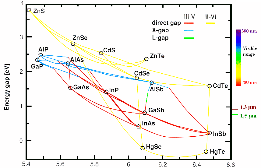
The first and most important one shows the bandgap
vs. the lattice constant
plus information about the gap type. It is shown below, with the II-VI compounds included for good measure: |

Lattice Constant (Å)
|
|
 |
There is a tremendous amount of information in this diagram (note that "X-gap"
and "L-gap" both denote indirect band gaps at the respective positions in the band diagram): |
|
 |
Most III-V compounds radiate at wavelengths above the visible region, i.e., in the
infrared. However, adding some Al to GaAs, producing AlxGa1-xAs, will shift the
wavelength into the red region of the spectrum – here are our red luminescence diodes and lasers! |
|
 |
Very fortunate: GaAs and AlAs have almost
the same lattice constant; we can thus combine (e.g., in a stack of layers) any mixtures of these materials without encountering
mechanical stress. |
|
 |
Very unfortunate: There are no
III-V compounds in the diagram that emit blue light – which is a severe
problem for many potential applications. While in the past, SiC could be used to some extent, it was only with the
recent (early 1990s) advent of GaN that this problem was solved. |
|
 |
SiC and GaN crystals, however, are not of the "zinc-blende" type common to all the III-Vs in the diagram but have a hexagonal
unit cell. They therefore do not easily mix with the others! To grow GaN layers
(bulk crystals can hardly be produced!) it is therefore favorable to use a hexagonal substrate as, e.g., SiC, Al2O3
(sapphire), or Si(111), plus a special buffer layer. |
|
 |
If we want to radiate at 1.3 µm or 1.5 µm – infrared wavelengths
of prime importance for optical communications – we should work with combinations of GaAs, InAs, and
InP. |
|
 |
Most interesting: The II-VI compounds are all direct
semiconductors and span a much larger range of wavelengths than the III-V's. The fact that they are not much used
for products tells us that there must be big problems in utilizing these compounds for mass products (prominent exception:
thin-film PV modules made of CdTe). |
 |
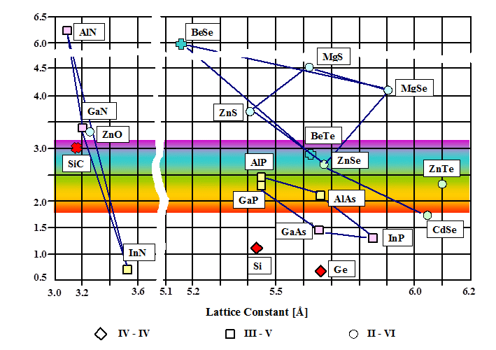
Here is another picture of the same thing including more materials: |
|
|
|
 |
In the left part, all hexagonal materials are shown; for them, the value of the in-plane lattice
constant (i.e., the one perpendicular to the hexagonal axis) is used. |
|
 |
The group-III nitrides AlN, GaN, and InN span an extremely wide range
of band gap energies, thereby providing a plethora of design opportunities for devices. In the first two decades of the
21st century, there were a lot of activities in this field, and the development still goes on. |
|
 |
The success in this field is mainly due to two basic achievements: First, to find out how
stable p-type doping can be reached; second, to find out how the materials can be grown with sufficient quality regarding high purity and low defect density, especially dislocation
density (that's one of the reasons the special buffer layer mentioned above is needed for). |
|
 |
The first problem was overcome by Shuji Nakamura, the second one by him and by Isamu Akasaki
and Hiroshi Amano. Together, they received the 2014 Nobel prize in physics. The Nobel lecture given by Nakamura ("Background Story of the Invention of Efficient InGaN Blue-Light-Emitting Diodes") provides valuable
insight into present-day semiconductor research and device development. |
|
 |
Zinc oxide has already found many different applications, but only very few in the
field of electronics. This is mainly hampered by the same difficulty originally also faced for the nitrides: Stable p-type
doping is still a problem. Nevertheless, ZnO-related research and development in other fields of materials science
is also very interesting; see, e.g., the relevant activities in the group of Prof. Adelung here at the TF. |
|
 |
In addition, among the group-III nitrides there is also BN, showing some similarity
to carbon: The most stable form is graphitic boron nitride (i.e., covalently bonded hexagonal layers kept
together by van der Waals forces), whereas the cubic modification c-BN (having zinc-blende structure) is metastable,
just like diamond. Graphitic BN has a band gap of 5.2 eV, it is mainly used as a lubricant (c-BN: 6.4 eV, used as
abrasive). |
© H. Föll (Semiconductors - Script)

