| Here is an actual research paper describing the ELYMAT technique | ||
New Developments of the ELYMAT Technique
J. Carstensen, W. Lippik, S. Liebert, S. Köster, H. Föll
University of Kiel, Faculty of Engineering,
Kaiserstr. 2, D-24143 Kiel
The ELYMAT technique is now routinely used for the monitoring of wafers and processes in the semiconductor industry, and no problems are encountered as long as the regular modes are employed with standard wafers. Extension of the technique to either non-standard Si (e.g. multicrystalline solar Si) or to more involved measurements have been proposed, but experiments were only partially successful. Applying a deeply penetrating Laser, a new mode is possible, yielding measurements which are completely independent of the surface condition and offer an improved signal to noise ratio. Combining several independent measurements as input in a mathematical model of the wafer allows to extract maps of the surface recombination velocity on both sides of the wafer and to obtain some information about the depth dependence of the diffusion length. Improvements in hard- and software of the ELYMAT allowed for the first time to obtain diffusion length maps with very high spatial resolution of multicrystalline Si. In addition, first experiments relating to a leakage current mapping will be presented.
1. Introduction
Life-time mapping techniques are by now routinely used by many producers of Si wafers and are finding their way to the factory floor of "wafer fabs", i.e. factories which the manufacture integrated circuits /1-8/. It can be surmised that this characterization technique was instrumental in improving wafer production techniques to a point where diffusion lengths of several mm are common, thus not only improving wafer quality and device yields in general, but also opening the way to novel etching techniques using very special electrochemical procedures /9, 10/.
The ELYMAT technique (for basic descriptions see /1, 2/) has been a strong contender among the methods employed, despite the fact that some properties of the ubiquitous Si-electrolyte contact are not well understood, e.g. the degradation of the interface after repeated measurements /11/. On the other side, the full potential of the ELYMAT technique /5-8/ has not been exploited either.
This paper reports on some new developments of the technique. It will be shown that by using Lasers of different penetration depths, a set of several measurements may be used to obtain depth information about diffusion lengths and to generate maps of the surface recombination velocity on the front and back side of a wafer. A particularly useful new mode (BSC: "both side mode") allows not only to overcome any problem with still existing surface recombination or degradation, but offers unparalleled signal to noise ratios and reveals new structures in wafers which so far have been hidden in the general noise level.
The diffusion length is not only a very important parameter in the integrated circuit industry, but the key parameter in any kind of crystalline Si intended for solar cells. However, so far it has been difficult to transfer life time mapping techniques to multicrystalline Silicon. By constructing a new cell and by optimizing measurement procedures, the successful application of the ELYMAT technique to multicrystalline Si has now become possible, results (including Lock-in techniques) will be presented.
The integral leakage current in the ELYMAT is known to provide important information about defects in the space charge region. First results of a mapping technique for leakage currents using an simple electrochemical method will be reported.
2. Development and Results of Three-Dimensional Diffusion Length Mapping
With regard to gettering techniques it would be advantageous to know the depth dependence of the diffusion length: L(z). Another parameter gaining in interest for submicron structures is the surface condition, e.g. the surface recombination velocity S(x,y) /12/. A minimum requirement for 3D-mapping would be to measure S(x,y) at both surfaces of the wafer and to determine the average L(x,y) for the front, center and rear part of the wafer separately. This implies knowledge of the approximate thickness of these three regions, i.e. the quantities z1 and z2 which define the boundaries of the center portion of the relevant wafer. In other words, at least seven independent quantities need to be determined at every point (x,y) of the wafer, which demands at least seven independent measurements. In practice, it is advisable, if not unavoidable to provide more than seven measurements, because the stability of the underlying model with respect to small variation in the data may be ascertained only if redundant information is available.
A minimum requirement for 3D mapping are measurements with two quite different penetration depths, i.e. Lasers with two different wavelengths. This allows for a couple of more or less independent measurements, since every wavelength can be used in four ways: Backside photo current (BPC) and frontside photo current (FPC) by illuminating the polished side of the wafer, and the same two measurements "upside down", i.e. illuminating the backside of the wafer.
Measurements using wavelengths of 820nm and 1047nm (with corresponding penetration depths of 16µm and 500µm) were duly undertaken and fitted to a model that contained the seven parameters given above. Results, however, were unsatisfactory. What was needed was some kind of "reference" measurement with results not depending on all seven parameters to be fitted and which minimized experimental scatter. The new "both side mode" provides exactly this reference and shall be described first.
The basic idea is simple: If a deeply penetrating Laser is used, the electrolyte junctions on both sides of the wafer can be biased to reverse conditions, front- and backside currents thus can be measured simultaneously. (This mode does not work with small penetration depths because in this case the backside current is too small to be measured accurately). The advantage of this mode is its absolute independence of S (mathematically S approaches infinity); this mode therefore intrinsically overcomes any problems with surface conditions, including degradation phenomena. There is yet another advantage of the both side mode, if one forms the relation between the two currents measured, i.e. IF/IB. By doing this, noise causing factors cancel, e.g. the Laser intensity variations; the picture thus obtained offers the perfect reference for any modelling endeavors. A minor disadvantage is the somewhat more complicated relation between the currents measured and the diffusion length.
Fig. 1 demonstrates this. Fig. 1a,c compare the two standard modes of the ELYMAT in this particular case. As usual, the FPC mode shows little structure whereas the BPC mode shows some features which would be interpreted as L-variations in the bulk of the wafer. Independent FPC and BPC measurements using a deeply penetrating Laser show these features in both modes as would be expected. The both side mode (Fig. 1e,f), however, is strikingly different:
Whereas the frontside current reproduces the features seen in the other measurements, the backside current picture reveals completely different circular structures not seen in any other mode. This implies that the prominent features seen in Fig, 1b-e are due to L-variations in the front part of the wafer whereas the rear "half" is differently structured.
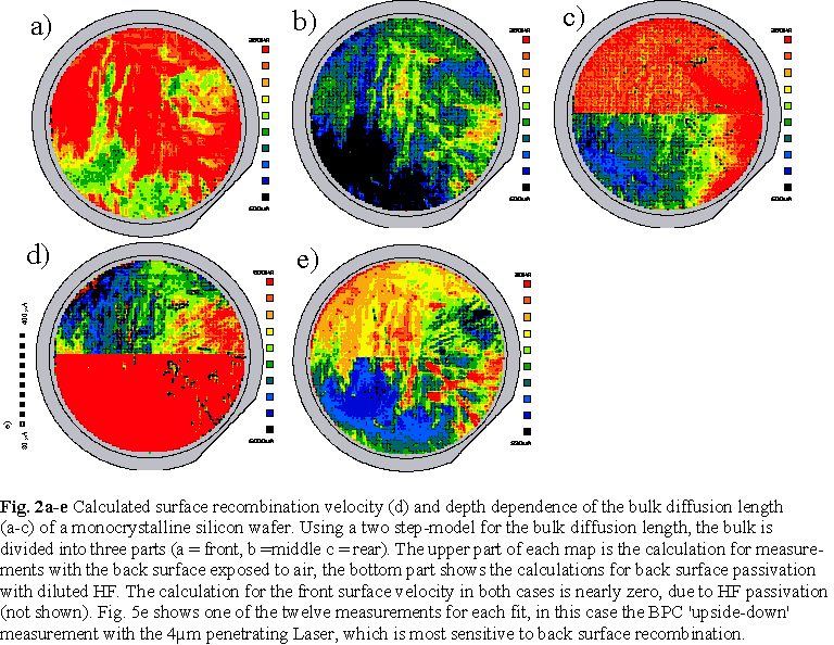
This is verified by the calculated depth dependence demonstrated in Fig. 2. The structures, seen in Fig. 1b-e correspond to the structures in Fig. 2a which is the calculated diffusion length for the front part of the wafer. The upper and lower part of these maps are calculated from different sets of measurements, one with the back surface exposed to air and another with the back surface passivated by HF. The difference in surface recombination is most obvious in the "upside down" BPC-maps (Fig. 2e) and the reduction of the surface recombination by HF-passivation is revealed in the calculated S-map (Fig. 2d). While the calculated diffusion length of the back part of the wafer is different for both measurements (probably due to different injection levels) the calculated L of the central and front part (Fig. 2a,b) are totally independent of the different boundary conditions, which is a good test for the validity of the fitting routine.
3. Measuring of Multicrystalline Silicon
Multicrystalline silicon (mc-Si, i.e. course-grained Si) becomes a propitious alternative to monocrystalline silicon in solar cell fabrication although the mc-Si solar cells still have a lower efficiency than mono silicon solar cells. Because the fabrication processes are identical for mc-Si and mono-Si solar cells, the reduction of efficiency is due to the as-grown material and research is required to improve this material. Since the ELYMAT technique is a powerful tool for monocrystalline silicon investigation, it was near at hand to apply this technique to mc-Si. Three problems, however, not encountered with mono-Si had to be solved: Breakage, leakage currents and high series resistance.
Multicrystalline silicon is cut into squared wafers of about 300 µm thickness which are much more susceptible to mechanical breaking than mono-Si. In the ELYMAT technique the critical moment for breakage is the closing of the electrolytical double cell. The double cell has to be leak-proof and square, causing some additional problems in comparison to mono-Si. The problems were solved by a fine tuning of mechanic and part of the cell and by using a flat metal ring as middle contact instead of the pointed needle contacts of the standard ELYMAT.
The leakage current (of the Schottky-like electrolyte contact) is orders of magnitudes larger than in mono-Si, due to defects in the space charge region (SCR) like grain boundaries, point defects and stacking faults. Thus the leakage current Idark is of the same order or ever larger than the light generated minority current Iphoto. The sum of both currents Ilight is measured by the ELYMAT technique. Calculating the difference
(1) ![]()
yields a small signal to noise ratio for the photo current on mc-Si. Experiments show that the dark current exhibits not only statistical fluctuations around an average value, but also sudden leaps between different dark current levels. Best results for the photo current are achieved using a procedure which smoothes the statistical deviations around the actual dark current level. Eq. (1) also implies that currents should be subtracted, which have been measured applying the same bias across the space charge region USCR. The measurements, however, are performed by applying a constant bias Ubias across the whole electrolytical double cell. Taking into account the series resistance UW of the system, USCR is a function of the current and the series resistance UW . The measured current values have to be corrected by a IR-compensation using the equation
(2) ![]()
and the above discussed statistical analysis of the dark current allows to measure diffusion lengths on mc-Si, where the standard ELYMAT dark current treatment fails.
Because of the inhomogeneous diffusion length distribution of mc-Si a high spatial resolution is needed in order to get satisfying information about the material structures (BPC resolution » wafer thickness, FPC resolution » influence area of grain boundaries = diffusion length). For FPC measurements a standard step width of 1/6 mm is chosen, leading to maps with 250000 pixels on an 85x85 mm area of the wafer. Measurements with higher spatial resolutions are possible with a step width down to 50 µm.
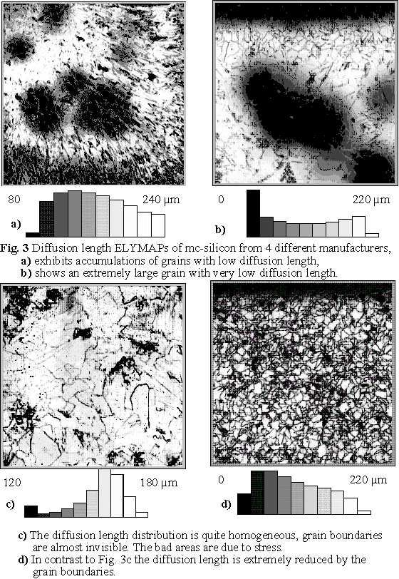
The four ELYMAPs in Fig. 3 demonstrate the capability of the ELYMAT technique for mc-silicon wafers. They reveal essential differences between the mc-Si material of four different manufacturers. Most obvious are the differing influences of the grain boundaries on the diffusion lengths. While Fig. 3a indicates a gettering effect of grain boundaries and thus an increased diffusion length, Fig. 3c shows a negligible influence of boundaries on L and Fig. 3d exhibits a high recombination near the grain boundaries.
4. Lock-in Technique
The Lock-in technique (phase sensitive measurement of a modulated signal) is generally used to tackle problems with a small signal to noise ratio. In the case of the ELYMAT technique this implies the measurement of photo currents generated by modulated Laser light. The Lock-in technique offers conceptive advantage for wafers with high leakage currents (e.g. mc-Si for solar cell application or non standard wafers like sand blasted silicon or highly doped material), in the case of low Laser intensity (injection level spectroscopy or measurements in the low injection regime) or if the photo current is very small (due to small diffusion length or in the IR-Bothside mode).
Applying a Lock-in technique for ELYMAT measurements, however, needs an understanding of the dynamical properties of the silicon electrolyte contact. While the dynamics of the minority current flow within the silicon wafer is well described by the diffusion equation, the dynamical response of the silicon electrolyte junction for modulated carrier concentration is not well understood. Impedance spectroscopy (modulation of the bias across the junction) shows a limiting frequency of about 1 kHz due to several capacitors across the silicon electrolyte contact (e.g. space charge region, Helmholtz layer). However, measurements in the FPC mode show no reduction of the Lock-in signal up to 10 kHz. So obviously the relaxation times of the chemical reactions are smaller than the relaxation times for the diffusion and do not limit the frequency for Lock-in measurements in the ELYMAT technique.
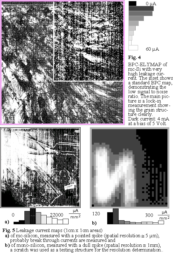
Despite the fact that there are some problems left concerning the quantitative analysis of BPC-ELYMAPs with Lock-in technique, the first results are very promising. Fig. 4. shows the amplitude map of the Lock-in signal on mc-Si. In contrast to the standard BPC-map (inset), the Lock-in signal shows the grain structure very clearly, although the wafer had extremely high leakage current.
5. Leakage current mapping
One of the more challenging tasks in characterizing Si is the development of a method for leakage current mapping. As Bergholz /6/ has shown, the integral leakage current of a wafer as measured by the ELYMAT may provide the most sensitive information about beginning contamination in a production line. For solar cell Si, high leakage currents are tied to reductions in the open-circuit voltage and are instrumental in reducing yields of solar cells.
Using an open electrolytical chamber with the silicon wafer as the bottom and filled with diluted HF, a scanned needle (counter electrode) allows to measure a leakage current with sufficient spatial resolution, if all parameters are optimal. This resolution depends on several parameters like needle geometry, HF concentration, the distance between needle and silicon surface and the applied reversed bias. In Fig. 5 two leakage current maps are shown with extremely different parameter sets. The current densities in Fig. 5b correspond to expected values from the measurement of the integral leakage current. Due to the dull shape of the needle the spatial resolution is not high enough to investigate e.g. crystal defects in mc-Si. This is possible by using a pointed spike (cf. Fig. 5a), but the measured current densities are far too high to be a part of the normal integral leakage current. This effect is presently not well understood, but probably due to the very inhomogenous electric field distribution which may induce local break through at defects in the SCR.
6. Conclusions
The utilization of new ELYMAT modes and measuring techniques offer new applications and increased measuring range, e.g. for depth dependence of diffusion length and surface recombination velocity or injection level spectroscopy. Another encouraging feature of the silicon electrolyte contact is the mapping of leakage currents, a material parameter which was up to now only measurable as an integral value.
References
/1/ V. Lehmann, H. Föll, J. Electrochem. Soc., 135, 2831 (1988)
/2/ H. Föll, Appl. Phys. A, 53, 8-19 (1991)
/3/ L. Jastrzebski; in "Semiconductor Silicon/1990" (eds. H. R. Huff et. al.), Electrochem. Soc., p. 614 (1990)
/4/ F. Shimura, T. Okui, T. Kasama; J. Appl. Phys. 67, 7168 (1990)
/5/ H. Föll, V. Lehmann, W. Lippik in: "Crystalline Defects and Contamination: Their Impact and Control in Device Manufacturing", Electrochem. Soc. Proc. Vol. 93-15, p. 252 (1993)
/6/ W. Bergholz, D. Landsmann, P. Schaubert, B. Schoepperl in: "Crystalline Defects and Contamination: Their Impact and Control in Device Manufacturing", Electrochem. Soc. Proc. Vol. 93-15, p. 63 (1993)
/7/ M. L. Polignano, C. Bresolin, F. Cazzaniga, G. Queirolo "Metal Contamination in Ion Implantation Processes", X International Conference on Ion Implantation Technology , Italy (1994)
/8/ P. Eichinger, J. Hage, D. Hubert, R. Falster in: "Crystalline Defects and Contamination: Their Impact and Control in Device Manufacturing", Electrochem. Soc. Proc. Vol. 93-15, p. 240 (1993)
/9/ V. Lehmann, J. Electrochem. Soc. 140, 2836 (1993)
/10/ S. Ottow, V. Lehmann, H. Föll, to be published
/11/ D. Walz, "Caracterisation de la contamination metallique dans le silicium par methodes de duree de vie application au cas du fer dans le silicium de type p", Ph.D. thesis, Grenoble 1995
/12/ J. Carstensen, W. Lippik, H. Föll; in "Semiconductor Silicon/1994" (eds. H. R. Huff, W. Bergholz, K. Sumino), Electrochem. Soc., p. 1105 (1994)


![]() 3.1.1 Silicon: General Properties and Technologies
3.1.1 Silicon: General Properties and Technologies
© H. Föll (Semiconductors - Script)