Doping and Mobility
 |
Shown are some standard diagrams (without detailed comment
at present) |
|
 |
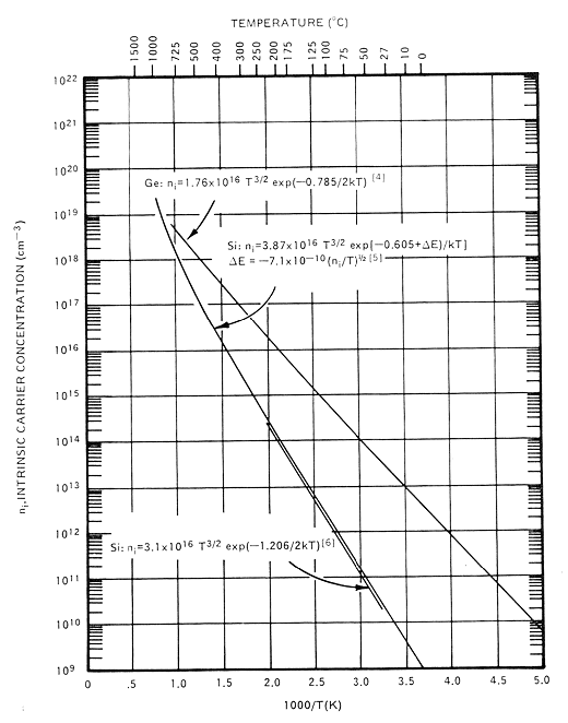
The first graph gives an Arrhenius
representation or Arrhenius plot of the intrinisc carrier
concentration in Si and Ge for various approximations. The (small) effect of the T3/2
factor can be seen for Ge; it is reponsible for the bending of the rather straight line at high temperatures. |
| |
|
 |
The next plot shows the intrinsic carrier concentration
of several semiconductors
as a direct function of the temperature. Note that at room temperature there is a difference of about 7 orders
of magnitude. |
| |
|
 |
This plot shows the dependance of the mobility on doping |
| |
|
 |
Here is the dependance of the mobility on temperature
in the interesting T-range for Si |
| |
|
 |
This is the combined result of carrier concentration and mobility:
The resisitivity of Si as a function of doping for electrons and holes separately. |
| |
|
 With frame

 3.4.1 Junction Diodes
 2.2.2 Doping and Carrier Density
 3.3.2 Scaling Laws
 Band-Bending and Surface Charge
 Solution to 3.1.1
© H. Föll (Semiconductors - Script)

![]() 2.2.2 Doping and Carrier Density
2.2.2 Doping and Carrier Density ![]() Band-Bending and Surface Charge
Band-Bending and Surface Charge