Trench etching
Pore formation in silicon as a effect of Stress corrosion cracking
Trench etchingPore formation in silicon as a effect of Stress corrosion cracking |
|
| Trench etching in p-type
silicon with organic electrolytes in cooperation with the ISIT in Itzehoe |
||||
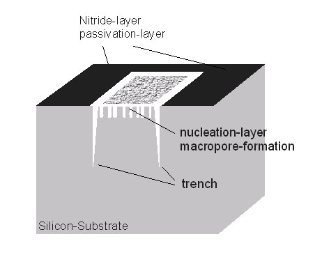
| On p-type Si wafers (10 - 20 Wcm, (100) orientation) nitride layers with varying thickness were deposited with a standard PECVD process and structured with standard lithographic processes. KOH pits were chemically etched. It has been shown that KOH pits can be used as starting points for macropores on p- and n-type silicon. The free silicon surfaces were defined with the nitride windows for etching random p-type macropores and arrays of pits for prestructured macropores. Pore etching was performed in an electrochemical cell. A computer controlled all parameters of the measurement setup. The temperature of the electrolyte was constant at 20°C. The electrolyte consisted of 4 wt.-% HF in organic dimethylformamide (DMF). Galvanostatic experiments with current densities between were performed | ||||
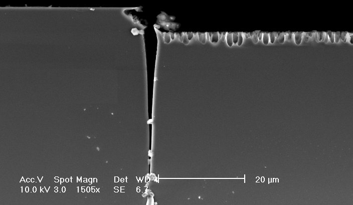
| Prestructured macropores in p-Si were obtained. A new kind of pores (dubbed "trenches") which is sensitive to mechanical stresses and which has the potential to generate deep trenches was found. | ||||
| The trench formation is connected with a minimal under-etch of the nitride-mask. The trench grows parallel to nitride-layer on the silicon over several hundred micrometers. The trench width is decreasing with the distance from the surface: 5 - 1 µm. The growth rate of the trench is 10 µm/min, this means about 10-times higher than the macropore growth rate. The trench grows perpendicular to the surface in <100>-direction. In the nucleation phase of the trench also macropores are formed. | ||||
 |
||||
 |
||||
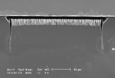
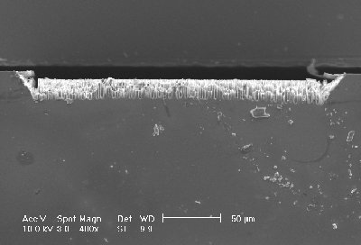
| Influence of the stress of the nitride mask. In the experiments only the thickness of the surrounding nitride mask is changed. | ||||
| thick nitride mask | thin nitride mask | |||
 |
 |
|||
| A series of experiments has been performed to investigate the driving force for the trench formation at the nitride edge. The results imply that the reason for the trench formation at the mask edge is a combination of mechanical stress and electric field strength effects at the trench tip. A nitride mask is known to induce severe stress in the silicon substrate which depends (nearly linearly) on the mask thickness. A series of experiments with masks of different thickness and an intermediate current density ( inducing trench as well as macropore formation) was performed. The micrographs above show how the results from two samples: The thicker nitride layer produces a larger trench in comparison to a thin layer. It thus may be concluded that mechanical stress induces preferential electrochemical silicon dissolution, probably due to stressed bonds. In a sense, trench formation could have some relation to the general phenomena of stress corrosion cracking, which is in fact so far unknown for electrochemical silicon etching with hydrofluoric acid containing electrolytes. | ||||