| |
macropores used for photonic crystals |
| The key-technique for 2D-photonic
crystals (Thesis of S. Ottow in the Group of H. Föll, 1996) |
|||
| The experimental setup for macropore growth is shown in the left figure and the principle of macropore etching is shown in the right figure, respectively. Photogenerated minority carriers (in the case of n-type Si this means "holes") diffuse from the back side of the sample to the pore (etch) pits and promote dissolution there, because of the enhanced electrical field in the space charge layer (SCL). The photographs show some examples of pore arrays obtained with this technique. We use two arrays, which differ in diameter of the pores, the pore spacing and the geometry (othogonal and hexagonal, the last with a closer package of pores). | 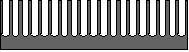 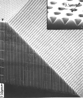 Step 2 |
||
| The next process step is to close the pores. This is necessary for for the definition of the microstructures with a photolithographic process. But before that a CVD Si3N4 passivation layer is deposited. We will see in paragraph 4 why this is important. The pores are closed with aluminum, which is evaporated on the top of the sample. This material was choosen because of its good stability for instance against plasma etching (see paragraph). The photograph shows that the pores are completely closed. Now it is possible to perform a photolithography to define the microstructures. After the photolithography the uncovered part of the aluminum mask is etched with phosphoric acid based etch. | 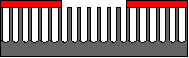 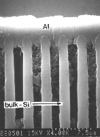 Step 3 |
||
| In addition one can see in the next two photographs on the right why the Si3N4 passivation layer is necessary. In the top picture the etching is performed without any passivation and the typical isotropic etch profile is obtained. By using the passivation the etch profile in nearly anisotropic and, in addition, the overall mask undercut is reduced twice. | 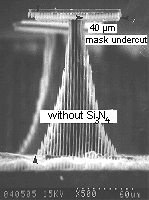 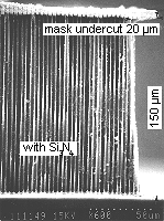 Step 4 |
||
| 2D-Photonic crystals | |||
| To fabricate photonic crystals suitable for near-IR and visible spectral ranges leads to the limits of today's technology due to a demanded regularity in the range of 10 nm. Electrochemical pore-formation of n-type silicon in hydrofluoric acid can lead to regularly patterned uniform pores with a diameter in the µm-range and a depth of several hundreds of micrometers [V. Lehmann, J. Electrochem. Soc. 140 (1993) 2836]. Based on this technique and the technique for mircostructuring from S. Ottow, an IR-photonic crystal was fabricated recently [U. Grüning, et al. Appl. Phys. Lett. 68 (1996) 747]. Optical measurements shows an photonic band gap. | |
||
| Point-defects can be studied with these structures. In the left picture a cavity for ligth is formed. | 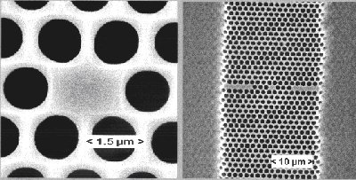 |
||
| see: F. Müller, A. Birnerm, U. Gösele, V. Lehmann, S. Ottow, H. Föll, Journal of Porous Materials, Vol 7, 1/2/3, S. 201 (2000) | 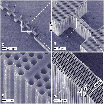 |
||
| With a periodic variation of the diameter of the macropores a quasi-3D-photonic crystal can be build. | 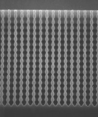 |
||
| 3D-photonic crystals | |||
| Macropores growth in the <100>- and the <113>-directions as a function of the substrate-orientation. If only <113>-pores growth a 3D-photonic-crystal can by build. | 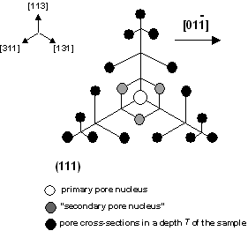 |
||
| In the picture is shown an non perfect 3D-photonic-crystal build by prestructred <113>-macropores on n-type silicon. The lithography-step was made by the MPI in Halle. The etching was done in Kiel. | 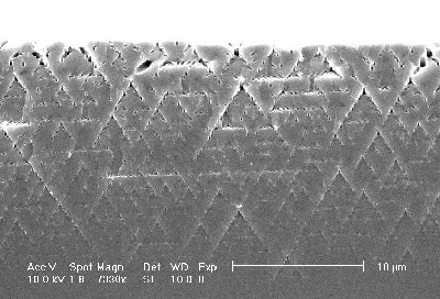 |
||
| This photograph shows an self.arrgement of <113>-pores in p-type-silicon. The self-arrgement leeds to a nearly perfect 3D-photonic-crystal. | 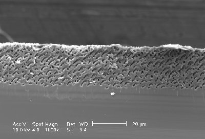 |
||