 Bias in
the HF-Si system Bias in
the HF-Si system
Bias in
the HF-Si system Bias in
the HF-Si systemApplying a bias across the elctrolytical cell there are two voltage drops; a first one across the Schottky-like silicon electrolyte junction and a second one due to ohmic losses in the electrolyte, the silicon and the needle-contacts.
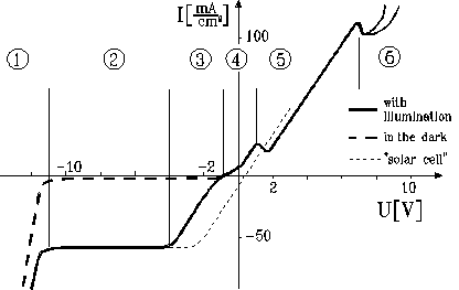
The IV-characteristic of p-Si
Using p-type silicon (p-Si) in the anodic region (upper right part of the IV-characteristics), the silicon has a positive potential to the counter electrode and majority carriers enter the SCR (forward bias condition). The current shows an exponential increase limited by the ohmic losses of the system (region 5). The two "peaks" are called PSL-Peak (PSL = Porous Silicon Layer) and oscillation-Peak (oscillations). Holes (h+) enter the silicon electrolyte junction and anodic etching occurs.
In reversed bias condition (cathodic region) electrons enter the surface and silicon is inert to etching. There is only a small leakage current (area 2 and 3 in the diagram and the dotted line), because of the depletion of the SCR. Illumination with laser light induces minorities carriers due to electron-hole pair generation. This leads to an additional photocurrent limited by the laser intensity (continous line in region 2). The ELYMAT normally works in this saturation regime where all minority carriers entering the SCR are measured as photocurrent.
Applying less bias (Region 3) the so called restricted photo current (RPC) is measured, which is a field of our actual investigation.