PDF-version of this document (1.4 BM)
13th European Photovoltaic Solar Energy Conference and Exhibition
ELYMAT TECHNIQUE ON MULTICRYSTALLINE SILICON FOR SOLAR CELL APPLICATION
J. Carstensen, W. Lippik, S. Liebert, S. Köster, H. Föll
University of Kiel, Faculty of Engineering,
Kaiserstr. 2, D-24143 Kiel
ABSTRACT: The ELYMAT (short for ElectroLYtical Metal Tracer) technique was originally designed as an inline tool for manufacturers of Si wafers and for wafer fabs to allow fully automated mapping of minority carrier diffusion length L [1-4]. Using electrolyte contacts and a scanned Laser beam, L-maps with high spatial resolution can be generated in a short time. Hard- and software has now beennewly developed to investigate multicrystalline silicon (mc-Si) produced for solar cell application. In designing the electrolytical double cell, the increased leakage current and the increased breakage probability of this material had to be taken into account. First investigations of mc-Si from different manufacturers with this new Solar-Elymat show considerable differences in the L-distribution. Especially the influence of grain boundaries on the mean diffusion length varies extremely, which is only seen on maps with a spatial resolution better than 0.20 mm.
1. THE METHOD
The "heart" of the ELYMAT consists of an electrolytical double cell, which is shown in Fig. 1. Filling both cells with diluted HF produces an electrolyte contact, which may be used as a Schottky-like contact, as an ohmic contact or as a surface passivating agent reducing the surface recombination velocity S to small values. A scanned laser beam generates minority carriers in the front part of the wafer. Reverse bias between the silicon wafer and the electrodes contacting the electrolyte allows to collect the photocurrent (cf. Fig. 2). Using a bias in the saturation regime of the IU-curve in Fig. 2, the photocurrent may be collected on the illuminated side (FPC-mode (Front-Side-Photocurrent)), on the opposite side of the wafer (BPC-mode (Back-Side-Photocurrent)) or even on both sides simultaneously (BSP-mode (Both-Side-Photocurrent)). In principle each of this photocurrent measurements allows to calculate the minority diffusion length, but in reality the different modes show distinct sensitivities to the diffusion length in the front or back half of the wafer and to remaining S. Thus the combination of measured photocurrents in different modes provides information on the depth distribution of the bulk diffusion length and the surface recombination velocity.
For routine measurements an infrared Laser (820 µm wavelength, 13 µm penetration depth) is used. The BPC photocurrent is very sensitive to the diffusion length L and the surface recombination velocity S at the front side. Assuming that the surface recombination velocity S of Si in contact with HF is negligible, the BPC is the standard mode for measuring L in the range from @ 0.2 to 3 times wafer thickness.
Using a Laser with a penetration depth greater than 0.3 wafer thickness, the BSP-mode allows an L-mapping totally independent of S. So if the surface is not perfectly passivated by HF or if we are interested in the surface-near L-distribution, the combination of independent measurement (BSP, BPC and FPC) allows to extract maps of the surface recombination or the surface near diffusion lengths [5, 6]. The number of independent measurements may be further increased using lasers with different penetration depth.
The FPC-maps supply additional information on the collection efficiency of the space charge region and the totally generated photo current. This mode almost equals that of a solar cell. A comparison of the FPC-maps with LBIC maps of completed solar cells allows to rate the efficiency of some production steps like anti reflex-coating, H-passivation or gettering.
2. APPLICATION ON MULTICRYSTALLINE SILICON
A number of hardware- and physical problems had to be solved to transfer the ELYMAT technique from circular monocrystalline silicon to square multicrystalline silicon (mc-Si). An electrolytical double cell had to be constructed taking into account the increased probability of mechanically breakage for mc-Si. Because of the increased leakage current (orders of magnitude greater than in mono silicon) the signal to noise ratio is reduced. The lateral inhomogeneous diffusion length distribution forces the use of a smaller scanning grid in order to get reasonable information on the mc-Si material, which increases the number of measuring points (about 250000 points per map). Only a technique with a short measuring time like the ELYMAT allows for such a high number of measuring points within a few hours.

Fig. 1: is a schematic plot of the electrolytical double cell of the ELYMAT. The silicon wafer is fitted between two half cells made of HF resistant material. The diluted HF electrolyte silicon junction serves as a schottky-like contact, while the middle contact of the Wafer should be an ohmic one. The front and the back circuit can be switched independently for the several ELYMAT modes. The laser beam is scanned by a x/y positioning system or by mirrors and is focused on the silicon surface to obtain maximum spatial resolution.

Fig. 2: shows the ideal current-voltage characteristics of the silicon electrolyte contact in comparison with normal solar cell. For p-type silicon the ELYMAT works in the negative bias region at saturation condition for the photo current. The schottky-like electrolyte-silicon contact builds up a space-charge region, which collects all reaching minority carriers. In real curves, the dark current is typically much larger and strongly voltage dependent.
3. THE MEASUREMENTS
Figs. 3 to 6 show diffusion length maps (calculated from BPC-measurements) of mc-Si from four different manufacturers.
These maps show strong differences in the homogeneity of the L-distribution and the influence of the grain boundaries on the diffusion length. In Fig. 3 and 4 the areas of small diffusion length are probably due to imperfect mixing of the ingot material and diffusion of the contamination while cooling down the silicon block. In Fig. 3 the contaminants have diffused through several grains, while in Fig. 4 there is one extremely large grain, which has only contaminated its adacent area.
The wafers 5 and 6 do not show these kinds of inhomogeneities. In Fig. 5 grain boundaries are almost invisible while Fig. 6 is dominated by the grain boundaries. The areas of reduced L in Fig. 5 are not correlated with the grain structure. They are probably dislocations due to stress, which has been introduced while cooling down the Si-block.
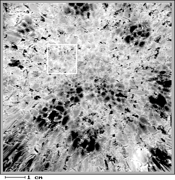
There is an extreme difference in the influence of grain boundaries on the mean diffusion length in Fig. 3 and Fig. 6 which hardly visible at the spatial resolution of the discussed maps. Therefore Fig. 8 and 9 show zooms of the marked areas in these maps. In contrast to Fig. 8, in Fig. 9 each grain boundary is surrounded by an area of increased L due to the gettering efficiency of the grain boundaries. The reduction of L due to the surface recombination velocity of the grain boundaries has to be compared with the increase of L by gettering in order to rate the integral influence of the grain boundaries on the mean diffusion length of a wafer.
The high spatial resolution is therefore a very important feature of the ELYMAT for characterising mc-Si. This resolution is not limited by the Laser focus but by the diffusion process itself. Fig. 7 and 8 show a 1.2cm x 1.2cm region of map 6 with a lateral resolution of about 50m m in the FPC- (Fig. 7) and BPC-mode (Fig. 8). Obviously there is a perfect correlation between the grain structure in those maps. The BPC-measurement is dominated by the diffusion length and shows a wide dynamic range, but the spatial resolution is limited by the diffusion of minority carriers through the wafer, i.e. the wafer thickness. The FPC-mode shows a much smaller dynamic range in the photocurrent and is sensitive to the collection efficiency of the front side. This mode shows the "real" spatial resolution of the ELYMAT.
4. SUMMARY AND CONCLUSIONS
The ELYMAT is a powerful tool for characterising Silicon. Using a Si-electrolyte-contact on both sides of a wafer and lasers with different penetration depths, a variety of independent photocurrent measurements is possible without any preparation of the wafer. This allows to calculate more than just one value for the diffusion length, but to distinguish between bulk and surface properties.
The most important features of the ELYMAT for characterising mc-Si are the high spatial resolution of this technique and the short measuring time, because many important aspects of the diffusion length distribution, e.g. the gettering efficiency of the grain boundaries, are only visible for a scanning grid smaller than 0.2 mm.
Fig. 3: BPC diffusion length map of an mc-silicon wafer. The measured area is 8.5cm x 8.5cm with a lateral resolution of 0.25mm. The diffusion length distribution is given as a grey scale from black (small diffusion length) to white (large diffusion length). The circular areas of low diffusion length cover more than a single grain and could be explained by an incomplete mixing in the melt. The grain boundaries increase the diffusion length because of their gettering efficiency.
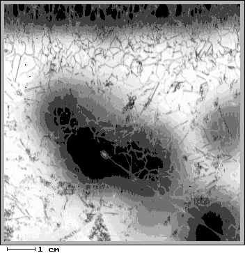
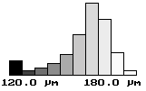
Fig. 4: BPC diffusion length map of an extremely inhomogeneous mc-Si wafer (8.5cm x 8.5cm). The bad area in the centre is due to one large, heavily contaminated grain. The diffusion of contaminants even reduces L in the neighborhood. The bad region at the top correspondents to the late stage of crystallization.
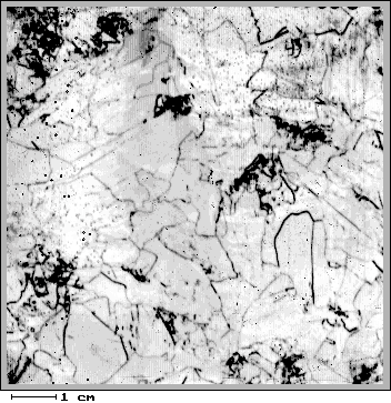
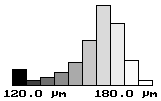
Fig. 5: BPC diffusion length map of an mc-Si wafer (8.5cm x 8.5cm) with very large grains. The diffusion length is quite homogeneous. Many of the grain boundaries have negligible recombination velocities. The dark areas of low diffusion length are probably due to dislocations introduced by stress during cooling down the silicon block.
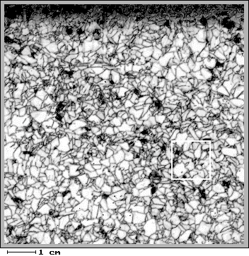
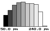
Fig. 6: BPC diffusion length of an mc-Si wafer (8.5cm x 8.5cm). There are many small grains surrounded by grain boundaries with a high recombination velocity, so the average diffusion length is small. This ELYMAP has the widest range in diffusion length of these four measurements.
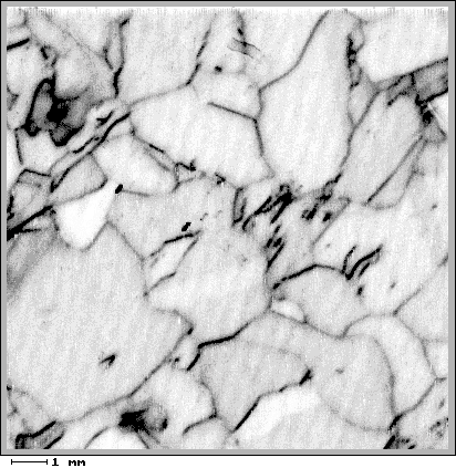
Fig. 7: This FPC photo current map shows the small region (1.2cm x 1.2cm) marked in Fig. 6 with a spatial resolution of about 50 µm. The FPC current measured with light of short penetration depth the highest spatial resolution of all ELYMAT-modes. It has low sensitivity to bulk properties of the silicon, but high sensitivity to surface near defects.
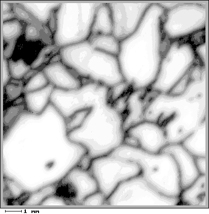
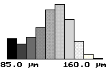
Fig. 8: The BPC diffusion length map of the same area as in Fig. 7 and the same scanning grid of about 50µm (160 000 pixels for these zooms). Because of the diffusion of the minority carriers through the wafer, the BPC ELYMAP exhibits a maximum resolution of approximately about 300 µm.
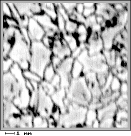
Fig. 9: A BPC zoom of Fig. 3 (marked square) showing the gettering efficiency of the grain boundaries. The resolution is in the magnitude of the wafer thickness (» 200 µm), the ELYMAP has 250 * 250 pixels. Like in Fig. 8 the grain boundaries have a high recombination velocity, but the grains themselves exhibit a gradiant in diffusion length from their borders (large diffusion length) to their centres (small diffusion length).
REFERENCES
[1] H. Föll, Appl. Phys. A53, 8 (1991)
[2] V. Lehmann and H. Föll. J. Electrochem. Soc. 135, 2831 (1988)
[3] H. Föll, V. Lehmann, G. Zoth, F. Gelsdorf, and B. Göttinger. In Proc. symp. Analytical Techniques for Semiconductor Mat. and Process Characterisation, ed. by B.O. Kolbesen, D.C. McLaughan, and W. Wandervort, 90-11, p. 44 (Electrochem. Soc., New York 1990)
[4] H. Föll, V. Lehmann, and W. Lippik. Proceedings. of ECS Conference of Crystalline Defects and Contamination, p. 252, Grenoble (1993)
[5] J. Carstensen, W. Lippik, H. Föll, Proceedings. "Semiconductor Processing and Characterisation with Lasers - Applications in Photovoltaics -", p. 159, Stuttgart (1994)
[6] J. Carstensen, W. Lippik, H. Föll, Semiconductor Silicon / 1994. H. Huff, W. Bergholz, K. Sumino (eds.), ECS Proc. Vol. 94-10, p. 1105, San Francisco (1994)