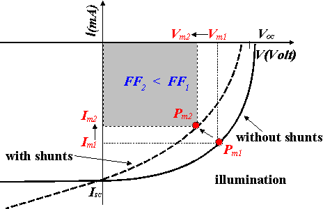
Figure 1. Shunts in the SC increase the leakage current and deteriorate most SC parameters like the fill factor FF, the efficiency h , the short-circuit current ISC and the open-circuit voltage UOC (m indicates the maximal power point)
PDF-Version of this file (200 kB)
PAPER REFERENCE. E9.3
A SIMPLE PASSIVATION
TECHNIQUE FOR THE
EDGE AREA OF SILICON SOLAR CELLS
IMPROVES THE EFFICIENCY
M. Hejjo Al-Rifai*, J. Carstensen and H. Föll
Department of Materials Science, Faculty of Engineering, Christian-Albrechts University of Kiel
Kaiserstrasse 2, D-24143 Kiel, Germany
________________________________________________________________________________
Abstract
The efficiency of silicon solar cells (SC) can strongly be degraded by localized defects especially at the edge of SC (e.g. scratches) which are introduced during the production of the SC and may cause local shunts. A new optimized chemical etching procedure has been developed which allows for a very effective passivation of shunts at the SC edges without reducing the surface area, i.e. without a reduction of the Isc current. In contrast to other techniques like plasma etching ("coin staking") or cutting off the edges, this procedure could be implemented cheaply in a large scale production.
The newly developed passivation method always leads to an improvement in the efficiency h of slightly or severely degraded SCs which is typically around 10%-30%, but can be as large as 100%, while good SCs are totally uneffected with respect to h while still showing an improvement of the leakage current.
Keywords: Edge Shunt Passivation, Efficiency Improvement
________________________________________________________________________________
1. Introduction
Many mass produced silicon SCs have defective p-n-junctions at their edges [1,2] which usually are introduced by the production process, e.g. after the diffusion of the emitter (doping process), after the formation of the front and the back contact (metalization), or after the deposition of the anti reflection coating.
These defects often act as local shunts and thus reduce the efficiency of the SC by increasing the leakage current and decreasing Pm,, Voc, FF and ultimately h (see Fig. 1 for the definition of the abbreviations) [1,2,3,4].
|
|
Figure 1. Shunts in the SC increase the leakage current and deteriorate most SC parameters like the fill factor FF, the efficiency h , the short-circuit current ISC and the open-circuit voltage UOC (m indicates the maximal power point) |
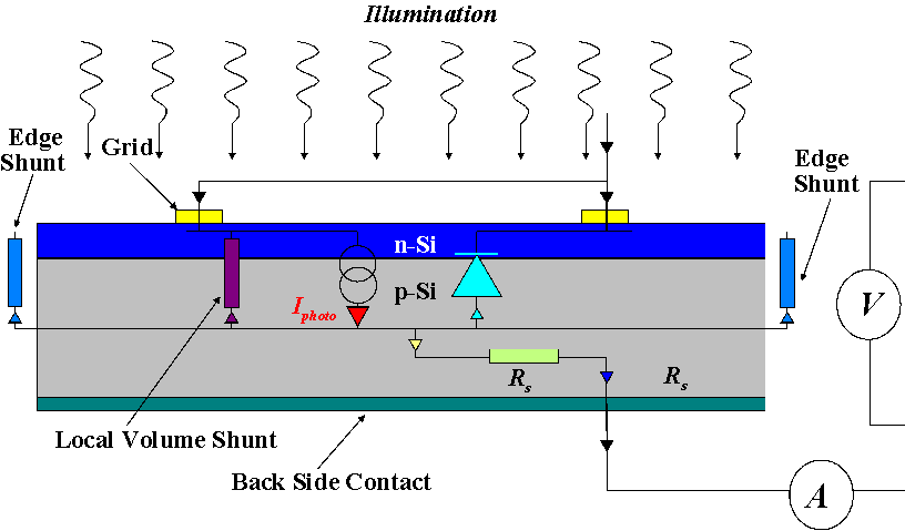
In this paper we will distinguish between volume shunts and edge shunts (Fig. 2). A non-representative statistic from our lab, obtained from the characterization of many SC (five sources of silicon SC; mono, multi-crystalline, and ribbon) by the new developed CELLO-technique [5,6], shows that about 80% of shunts in silicon SC are localized at the edge area and just about 20% are localized in the volume of SC. While both types of shunts can be passivated in principle, the passivation of edge shunts is the more pressing problem and practical, while the passivation of volume shunts is difficult and thus will not be discussed further.
|
|
Figure 2. Volume shunts and the edge shunts schematically shown in a in a SC circuit diagram. |
There are two known and practiced passivation methods for edge shunts in silicon SC. In the first one, the SC's are stacked and afterwards the edges are plasma etched. This technique (called "coin staking" [7,8]) is effective but quite expensive. In the second method, the edges are cut off with a diamond saw [2]. While this is a relatively cheap method, it reduces the area of the SC. The passivation method proposed here is potentially cheap, does not decrease the active area, and on occasion even improved the SC efficiencies of cells already passivated by one of the methods mentioned above.
2. The Passivation Method
It is well know that a hot alkaline solution like KOH allows to preferentially etch off defects in silicon and thus from SC's [5,9,10,11,12], and thus could be used to passivate defect induced shunts. However, just dipping the edges of a SC into hot KOH leads to substantial area losses because not only will the p-n-junction be removed in a region a few mm in width around the edge, but splashes of hot KOH and KOH vapor tends to destroy the AR coating in a sizeable part of the SC. The process is difficult to control and it is practically impossible to restrict it to the edges.
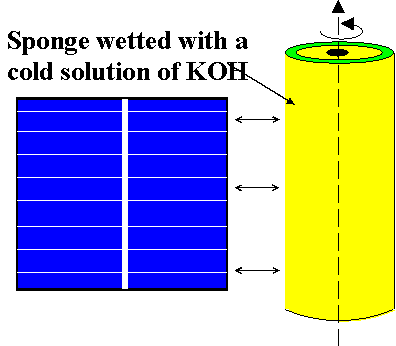
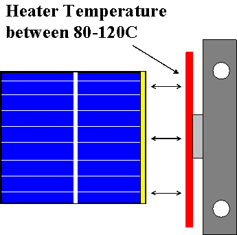
To avoid such problems for the defect etching responsible for edge shunts, a new KOH passivation technique has been developed. The key feature is to start with a cold solution of KOH (cf. Fig. 3). In a first step, one edge is wetted locally with the cold solution of KOH (10-30%), e.g. by using a sponge saturated with KOH (Fig. 3a). This allows to deposit a defined quantity of KOH on the edge area of the SC. In a second step the wetted edge is heated up locally for 20-25 sec by using e.g. a heating plate kept at (80-120)°C (see Fig 3b). The other edges are passivated in turn, or, with a somewhat more sophisticated set-up, in parallel. A simple cleaning step with distillated water may follow, but is not really necessary, because the KOH has completely evaporated. In the lab experiments, no degradation of passivated SCs has been found several weeks after the process if the rinsing procedure was skipped.
|
|
|
| (a) |
(b) |
Figure 3. A defined quantity of KOH is deposited at the edge area (a). The wetted area is heated up locally for about 20-25 seconds (b). |
|
This passivation procedure has been applied to several kinds of commercially available silicon SC (mono , multi crystalline and ribbon grown silicon SC) and the relevant parameters were measured before and after the passivation.
In particular, IV-characteristics were measured in the dark (yielding the leakage current) and under a (non-standard) illumination at a constant temperature of 25° C. In addition, in many cases "shunt maps", ISC maps, and UOC-maps have been measured by a newly developed technique called CELLO (short for solar CELl LOcal characterization [5,6]). The various maps allowed to follow the decrease of the shunt density at the edge after the passivation and to follow the improvement in essential SC parameters.
3. Results
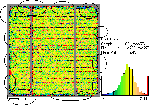
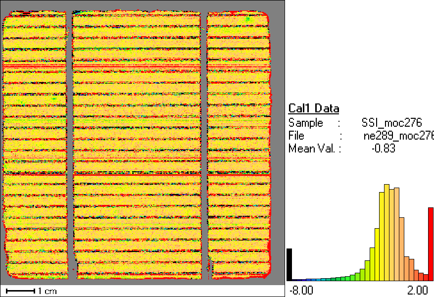
First results have been obtained from severely degraded, commercially available mono-crystalline silicon SC (10x10 cm2). The CELLO shunt-map of a typical SC before the passivation (Fig. 4a) shows strong edge shunts (black areas, much better visible in color coding). Most of the edge shunts have been removed by the passivation as shown in Fig. 4b.
|
|
|
| (a) |
(b) |
Figure 4. CELLO-maps show a number of shunts (black areas, some are marked by circles) at the edge of the SC before the passivation (a) which vanish after the passivation (b). |
|
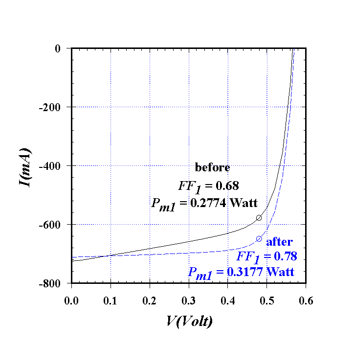
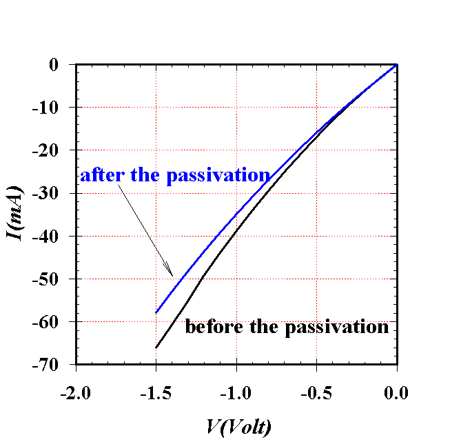
The reduction of the shunt density is clearly visible in the IV-characteristics, too (cf. Fig. 5a,b). Most SC parameters show a strong improvement; note that the fill factor increased from 0.68 to 0.78, i.e. by 15%. A slight reduction of the short circuit current Isc, indicating a small area loss, is well overcompensated by the other parameters: The (relative) efficiency of the SC after passivation increased by about 12%.
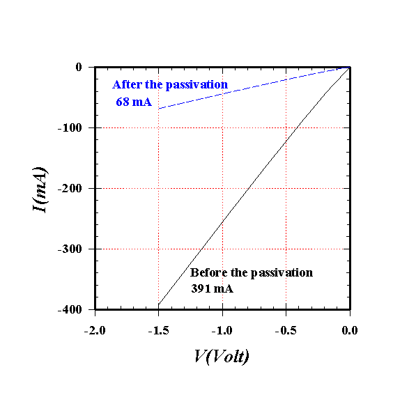
The leakage current in the dark is the SC parameter most sensitive to shunts. It therefore can be used as a sensitive (but with respect to the SC efficiency indirect) measure of the efficiency of a passivation process. In Fig. 5b the dark current in reversed bias is shown before and after passivation and a large improvement is evident.
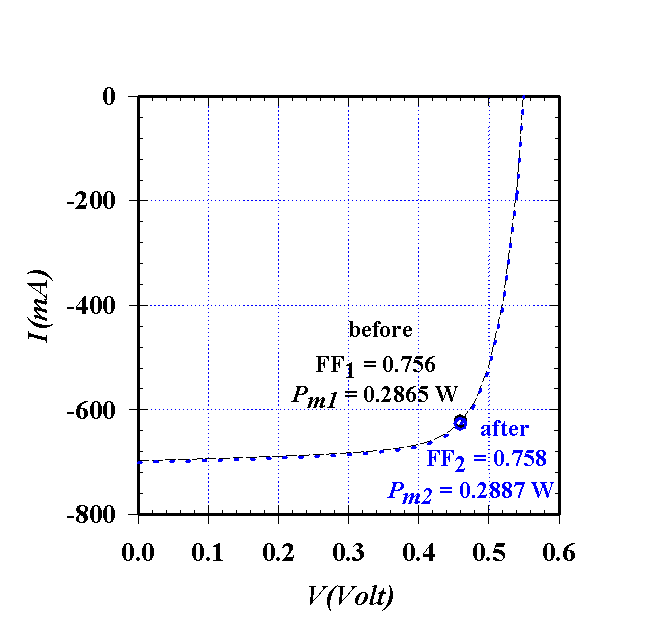
Since it might be unpractical in large scale production to only passivate SC's "with a problem", passivation methods should be useable with good SC's, too. In this case the performance cannot be improved and the practicability criteria is now that good SC's must not be degraded. The new passivation method therefore was applied to a very good mono crystalline silicon SC showing "ideal" IV characteristics and very low leakage currents. After passivation, the IV- characteristics under forward bias and illumination were unchanged (cf. Fig. 6a), while for reversed bias in the dark even a reduction of the leakage current resulted (cf. Fig. 6b)., meaning that even a good SC was made somewhat better. For almost all SCs passivated, a further improvement of the SC parameters was found after one or two days. Probably the native oxide which forms under ambient conditions further passivates the edge areas of the SCs.
|
|
|
| (a) |
(b) |
Figure 5. The IV-curves under illumination (a) clearly show the improvement of most SC parameters (12.5% increase in efficiency); the leakage current (b) is strongly reduced after the passivation. |
|
Similar results have been obtained for a large number of different silicon SCs (mono, multi crystalline and ribbon); in all cases improved SCs resulted. However, CELLO shunt maps showed that not all edge shunts are amenable to the passivation method; on occasion a few ones remained unchanged, i.e. unpassivated.
|
|
|
| (a) |
(b) |
Figure 6.The IV-curve under illumination (a) does not show any discernible changes for good SCs, but still an improvement in the leakage current (b). |
|
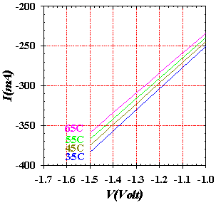
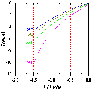
This "digital" behavior of shunts seems to be correlated to the temperature dependence of the leakage current induced by the shunts. While straight p-n-junction theory predicts that the leakage current must increase with increasing temperature, many real SCs with strong shunts show do not follow the theory: Their leakage current decreases with increasing temperature as illustrated in Fig. 7a. A simple correlation was found: The stronger this unusual temperature dependence, the more effective is the edge passivation. A SCs with a normal temperature dependence as shown in Fig. 7b (note the difference in scale!) could not be improved significantly any more by passivation. This implies that the edge shunt properties are responsible for the strange temperature dependence of the leakage current, and that they may be modeled as an essentially ohmic current path with a strong positive temperature coefficient.
|
|
|
| (a) |
(b) |
Figure 7. SCs which could be passivated effectively by the new method show a decrease of the leakage current with temperature (a); whereas the leakage current increases with increasing temperature for good SCs (b). Not the change ion scale between (a) and (b). |
|
4. Discussion
Edge shunts are a result of many process variables; information on their typical properties (nature, density, impact on SC performance, source) is usually unknown or not released by SC manufacturers. A passivation method thus must be able to remove at least the majority of shunts, must not do any harm to SC's without shunts, and, in order to be practical, must be cheap and applicable at an optimum point in the process flow, i.e. after the emitter diffusion or before the AC coating.
Obviously, it can not be checked in a laboratory environment, if all these conditions are met. However, considering the results obtained and the rather simple passivation procedure, one may state with some confidence that the integration of this passivation method into a production flow has a definite potential to yield improved SCs at little additional cost. An optimization relative to a particular process and starting materials is possible by using the CELLO technique and temperature dependent leakage current measurements for providing guidelines as to the nature, location, and amenability to passivation of the particular shunts encountered in the process.
Since the procedure works well with a large number of quite different silicon SCs it may be applicable for other types of SCs (e.g. thin films, GaAs) as well.
5. Conclusion
A new method for the passivation of edge shunts in silicon SCs has been developed. The method is effective, cheap, simple, and flexible and will either lead to an improvement, or leave the SC unchanged. Increases in the efficiency of commercial (albeit not very good) SCs of more than 100 % have been obtained and even very good SCs may still show some improvement of their leakage current. The method can be used in a preventive or in a selective mode. i.e. applied to all SCs in a production process, or only to selected "troubled" SCs. Shunt maps and measurements of the temperature dependent leakage current are very useful for the optimization of the passivation process.
References