MACROPORE-FORMATION ON HIGHLY DOPED
N-TYPE SILICON
M. Christophersen, J. Carstensen, and H.
Föll
Materials Science, Faculty of Engineering
Kaiserstr. 2, 24143 Kiel, Germany
Phone: + 49 431 77572-501, Email: hf@tf.uni-kiel.de
Using specially "designed" electrolytes, it is possible to obtain macropores even in highly doped n-type-silicon (0.020-0.060 Wcm) without illumination. Based on predictions of the "current-burst-model" [1], HF-containing electrolytes were systematically modified with strongly oxidizing components and evaluated with respect to their ability to produce macropores. Well developed macropores with depths up to 10 µm and pore-diameters between 200 nm and 2 µm could be obtained in several cases. The macropore pore nucleation starts with at facetting of the surface on {111} planes.
In 1990 Lehmann and Föll [2] discovered that very regular arrays of macropores with extremely large aspect ratios could be obtained in the n-Si/HF system. They explained the formation of these pores on the base of a so-called "space charge region" model, assuming that the current, photo-generated at the back-side of the specimen, is focussed on pore tips because of the bending of the space charge region around the tip. The model has some merit for the formation of macropores in n-type Si, especially for the regular pore arrays shown in [3], because based on this model and additional empirical results it is possible - within limits [4] - to produce pore structures as desired [5].
1994 macropores on p-type-silicon were found by Propst and Kohl [6] by anodic etching in a HF containing organic electrolyte (HF in water-free acetonitril). The authors explained the macropore formation in a mostly chemical way – the silicon dissolution was assumed to be a strong function of the crystal planes. The first more physical models for macropore formation on p-type-silicon assumed chemical passivation of the macropore walls via selective solvent molecules [7] or employed special effects due to the high resistance of the electrolyte and the substrate in the experiments performed so far [8]. Lehmann argued that the space charge region model used for n-type Si, if coupled with general diffusion properties, could also explain macropore formation on p-type-silicon [9].
Other models relevant to macropore formation are the "field induced break-through" model [10], which assumes that at some pore tips the electrical field strength is sufficient to allow avalanche break through which then generates the necessary carriers for further growth of the pore. Combinations of the space-charge-model and the break-down-mechanisms were used to explain the transition from macro- to mesopore-formation [11]. Models referring to e.g. pore wall passivation [7, 12], diffusion limited random walk [13], or surface instabilities give general scales for the pore-morphology under certain conditions [13, 14, 15, 16].
However, despite the plentitude of macropore formation models, a general agreement pertained that macropores grow only on low doped p- and n-type silicon [e.g. 11]. Reported limits for macropore-formation on n-type-silicon were ~ 0.1 Wcm [11] and on p-type ~ 10 Wcm [7].
A new model from Carstensen et. al. [1] (the theory will be given in detail in [17]), which claims applicability to all electrochemical phenomena of Si, is based on the assumption that the current-flow through the liquid-solid-interface is spatially and temporally inhomogeneous and might be seen as occurring in "current-bursts" According to this "current-burst-model", macropores form if the balance between direct dissolution and oxidation in a current burst is within a certain bandwidth, and mesopores, generally observed on highly doped p- and n-Si, are observed if the oxidation component is too small. Accordingly, an enhancement of the oxidizing power of an electrolyte, should have the potential to produce macropores under conditions where otherwise only mesopores occur.
Highly doped n-type specimens (resistance: 0.020-0.060 Wcm, CZ-grown, (100)-oriented and polished from MEMC) were used. The specimens were subjected to anodic etching under the following conditions: Galvanostatic current densities between 0.75-4 mA/cm2 (applied from an KEITHLY 238 high current source), stabilized electrolyte temperature (20°C), and no illumination of the sample. Four different types of hydrofluoric acid containing solutions were used: The solutions were based on (a) acetic acid, (b) TMAH (tetramethylammoniumhydroxide), (c) CrO3, and (d) H2O2.
Under open circuit conditions the purely chemical silicon dissolution for all solutions was investigated and found to be negligible at 20°C; this was checked by gravimetry. The silicon dissolution reactions observed thus were purely electrochemically in nature.
The pores produced were investigated with a scanning electron microscope (SEM). Plane view micrographs show the (100) plane, whereas after cleaving the samples, the (110) cleavage planes showed the pores in cross-section.
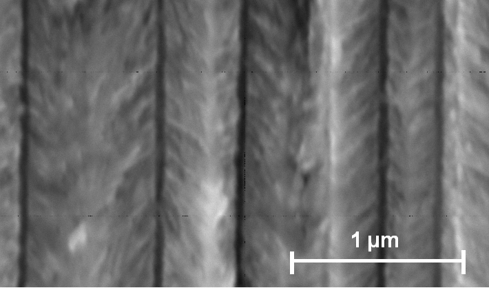
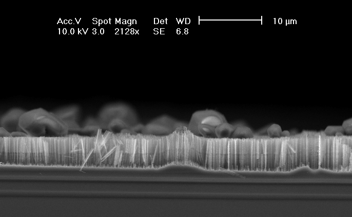
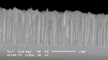
First, the behavior in HF – water electrolytes without oxidizing additions was checked in order to establish an unambiguous reference. The well known mesopores were obtained as expected [11]. The size of mesopores in n+/p+ Si is usually in the 10 nm region [11], but in [18, 19] mesopores with structure-size up to 100 nm were shown. In Fig. 1 a SEM-micrograph of a mesoporous layer obtained in our experiment on the 0.020-0.060 Wcm-n-type-substrate is shown. The main pores are <100>-orientated, a strong tendency to form branches is visible.
|
|
| Fig.1: SEM-micrograph: 4wt.-% HF (aqueous), 4 mA/cm2 for 60 min |
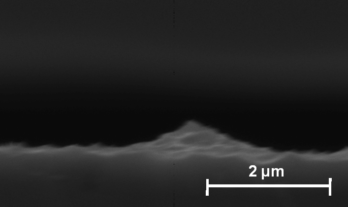
The dependence of the pore morphology on the HF concentration for the four electrolytes a - d has been studied in detail. Without hydrofluoric acid, the different solutions allow only anodic oxide formation. Increasing the HF concentration slowly (only the HF-amount is changed, all the other etching conditions were retained), the surface morphology changes significantly, especially in the TMAH-HF-system, on which we now will focus. Very low HF concentrations lead to a homogeneous dissolution (electropolishing) of the silicon with a rather smooth surface (interrupted occasionally by some protruding undissolved islands, cf. Fig. 2 a). By increasing the hydrofluoric acid concentration, the surface roughness increases and hillock formation can occur (Fig. 2 b) – c)).
|
|
|
Fig. 2: SEM-micrographs, cross-sections. 1.5 mA/cm2; 60 min 250 ml TMAH plus |
||
a) 1 ml HF |
b) 5 ml HF | c) 7 ml HF |
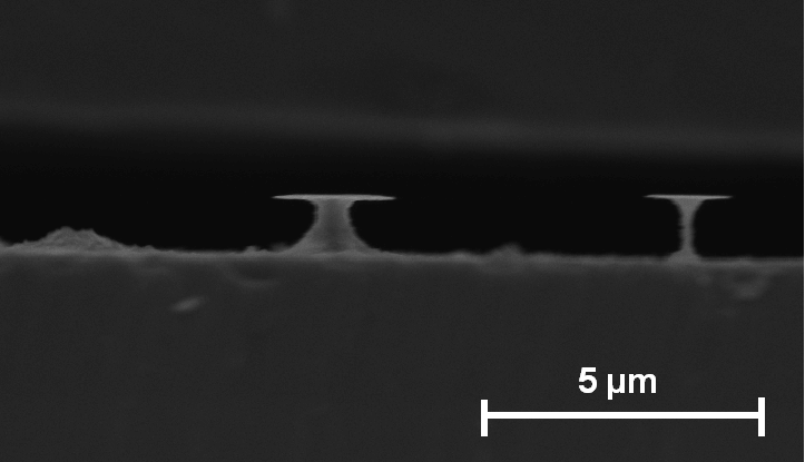
Upon increasing the HF-concentration even more, the surface roughness changes steadily to macropores; this is shown in Fig. 3.
|
|
|
Fig. 3: 12 ml HF in 250 ml TMAH, 1.5 mA/cm2, SEM-micrographs |
|
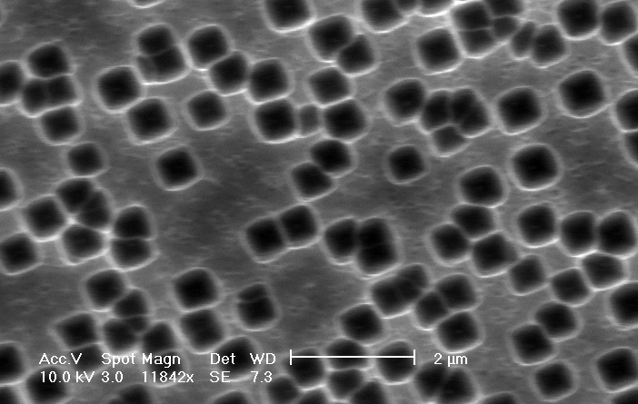
| a) Cross-section: Macropores with depth up to 5 µm and diameters around 1 µm are formed. |
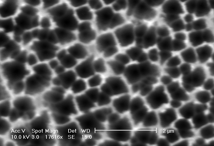
b) Plane view: The distance between macropores can be several micrometers. |
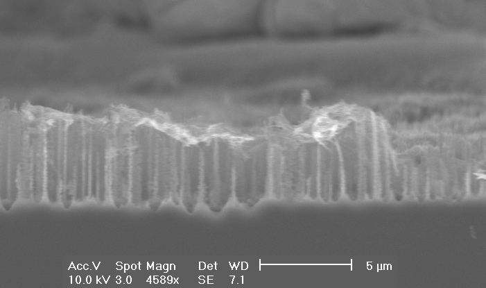
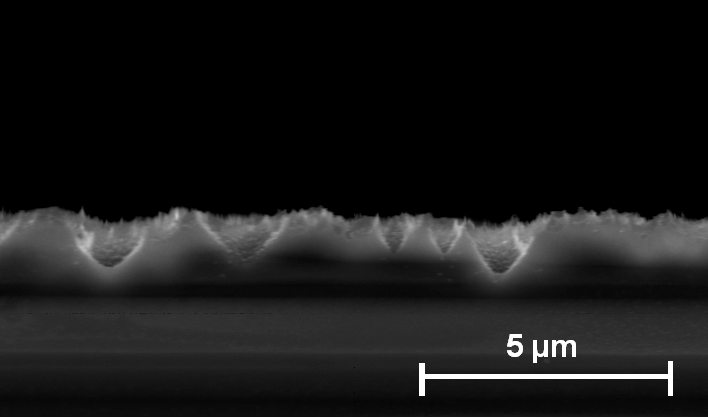
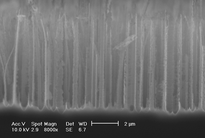
If the HF concentration is increased even more, the diameter of the macropores reduces steadily: In Fig. 4 a)-b) macropores with diameters of about 600 nm are shown. This is a significant reduction taking into account that the HF-concentrations have changed only from 5 to 6 percent. Mesopores, taken as pores with diameters £ 100 nm, start to grow at a HF-concentration of 8% or larger.
|
|
|
Fig. 4: SEM-micrograph, cross-sections. 15 ml HF in 250 ml TMAH, 1.5 mA/cm2 |
|
| a) Macropores with depth up to 10 µm and diameters up to 600 nm are formed. |
b) Overview: The macropore layer is highly uniform |
It can be concluded that the parameter window for stable macropore-growth on n+-substrates with respect to the electrolyte composition is quite small.
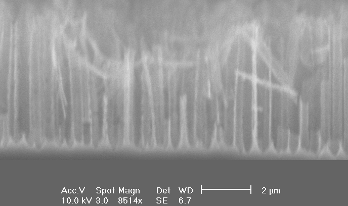
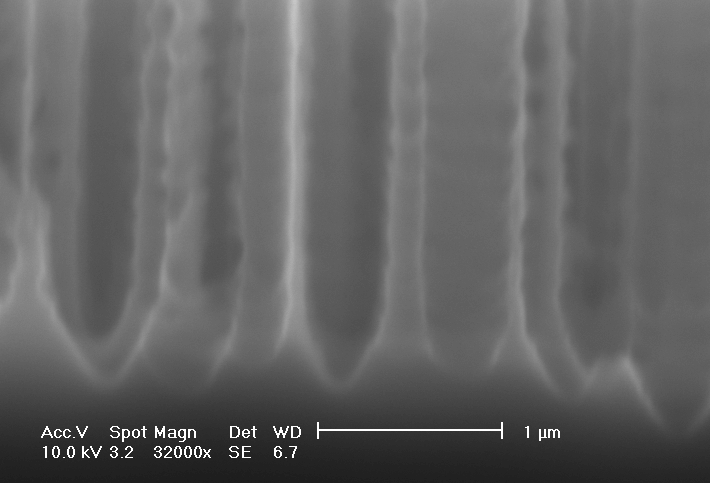
Next, we investigated the formation of macropores as a function of the current density. According to the current burst model, the area of electrochemical reaction (respectively the number of local bursts), is defined by the current density. Doubling the current density leads to an increasing number of macropores and not to a higher growth rate (see Fig. 5 a)-b)) in comparison to Fig. 4 a). The pore tips in Fig. 5 c) are still formed by (111)-planes.
|
|
|
|
Fig. 5: 15 ml HF in 250 ml TMAH, 3 mA/cm2 |
||
| a) Cross-section, SEM-micrograph: Macropores were formed. |
b) plane-view, SEM-micrograph: The current-density is doubled in comparison to Fig. 4, the pore density is obviously increased. |
c) Cross-section, SEM-micro-graph: 15 ml HF in 250 ml TMAH, 3 mA/cm2: The pore tips still show (111)-facets. |
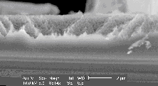
The nucleation of the macropores takes place at (111) facetted pyramid shaped pits in a generally rough surface, see Fig. 6 a). The (111) facets in the nucleation phase and at the pore-tips during stable growth may act as an additional stabilizing factor for the macropores, because of electric field strength enhancement at sharp structures. The holes needed for the electrochemical reaction without illumination must be generated somewhere; sharp pore tips are beneficial for this purpose.
 |
 |
| Fig. 6: a): Cross-section, SEM-micrograph: 15 ml HF in 250 ml TMAH, 1.5 mA/cm2: The nucleation of the macropores takes place at (111)-pyramids forming in a generally rough surface. |
Fig. 6:b): n+-type-silicon, 4 mA/cm2, 30 min etch-time, 8g CrO3, 10 ml HF and 200 ml H2O. Macropores were obtained, but less well developed compared to TMAH. |
TMAH is often used as a component for anisotropical chemical etching silicon etch [cf. 21], because it does not etch (111) planes. But the TMAH-HF-system is not the only mixture suitable to build macropores on n+-material, we obtained macropores in a mixture of 8g CrO in 10 ml HF and 200 ml H2O, too. Chromium oxide is known as an oxidizing reactant for silicon, it is the basic component of most defect etches, e.g. in the "Sirtl etch" [22] or "Secco etch" [23].
Generally, the "window" for macropore formation in n+-type Si, as expressed in the suitable region in parameter space, is quite small or non-existent for all electrolytes investigated (including some not mentioned here). In p+-type Si, it is either non-existent or as not yet been discovered in a quick survey performed in the context of this work. While this finding is not totally unexpected, it is, at present, open to speculation.
Discussion: To the best of our knowledge, this is the first time that macropores on n+-type silicon were obtained. Pore diameters up to 1 µm with pore-depth up to 5 µm could be produced. The distance between pores reaches several micrometers; but even more typical smaller distances below 1 µm are still well above the width of the space-charge-region (SCR) which is about ~10 nm for this highly doped material. This implies that the macropores are not primarily caused by SCR effects.
No backside illumination could be used because the small diffusion length of highly doped Si would prevent the hole diffusion to the front side. The holes needed thus must be generated by electric field effects (avalanche break-through) which is easy in highly doped materials. But avalanche break-through so far has been considered to be prime the effect for mesopore generation and thus should not be seen as a prime reason for macropore formation. According to
the current burst model, the prime reason for macropore formation in this (and other) cases is the decreased probability for current bursts on H-passivated surfaces coupled with the smoothing action provided by a minimum of oxidation following direct dissolution, and this accounts at least qualitatively for the experimental observations. Other factors, as, e.g., the shape of the SCR, or the supply of holes may influence macropore stability, too, by influencing the nucleation probability of current bursts, but the interplay between H-passivation and oxidation must be seen as the prime parameters.
The pore tips are formed by {111} pyramids, and the pore shapes tend to be quadratic (cf. Fig. 3b)) This can be seen as a remnant of the still very strong direct dissolution component prevalent in highly doped Si [19] which has been barely compensated by the oxidants to allow macropore formation. Since the (111) planes are known to have the fastest hydrogen passivation kinetics [1], they are least likely to nucleate current bursts and thus are always prominent as "stop planes" as long as the strongly anisotropic direct dissolution mode prevails in a current burst. It is known for TEM-investigations [20] that (111)-facets exists at the macropore walls in p- and n-type macropores which confirms the H-passivation mechanism for macropore wall passivation.
We interpret the observation of macropores in n+-type Si as an important confirmation of the hypothesis that macropore formation needs a minimum of oxidation. The strong anisotropic character of the TMAH etch may have an additional stabilizing influence by changing the H-passivation, one of the basic ingredients of the current burst model, in a favorable direction, too. This would be compatible with the model of Allongue et. al. [23] which correlates the anisotropy of purely chemical etches with the H-passivation of the silicon surface.
Conclusions: One of the basic assumptions of the current burst model [14] concerning macropore formation has been experimentally verified by inducing macropore growth in a systematic manner in n+-type Si where macropores have not been previously observed. According to the current burst model, macropores instead of mesopores should occur in highly doped Si if the direct dissolution part of a current burst could be augmented by adding a sufficiently strong oxidizing component. Several electrolytes with oxidizing tendencies were tried; some proved to be successful. A window, albeit small, exists in the balance of direct dissolution/oxidation for some electrolyte compositions which allows macropore formation as pre
dicted. Backside illumination and diffusion processes coupled to SCR can be excluded as additional stabilizing processes, and the dominant stabilizing component should be the H-passivation of the pore walls, possibly augmented by field-strength induced avalanche effects at the pore tips.
Acknowledgements:
We are grateful to Bob Falster form MEMC for supplying silicon wafers. This work was supported by the Deutsche-Forschungs-Gemeinschaft (Förderungsnummer: FO 258/1-2).
References:
[2] V. Lehmann, H. Föll, J. Electrochem. Soc., 137, 653 (1990)
[3] V. Lehmann, U. Grüning, Thin Solid Films, 297, 13-17 (1997)
[4] M. H. Al Rifai, M. Christophersen, S. Ottow, J. Carstensen, H. Föll, J. Electrochem. Soc., 147, 627 (2000)
[5] V. Lehmann, J. Electrochem. Soc., 140, 2836 (1993)
[6] E. K. Propst, P. A. Kohl, J. Electrochem. Soc., 141, 1006 (1994)
[7] E. A. Ponomarev, C. Levy-Clement, J. Electrochem. Soc. Lett., 1, 1002 (1998)
[8] R. B. Wehrspohn, F. Ozanan, J.-N. Chazalviel, J. Electrochem. Soc., 145 (8), 2958 (1998)
[9] V. Lehmann, S. Rönnebeck, J. Electrochem. Soc. 146 (8), 2968 (1999)
[10] M. J. J. Theunissen, J. Electrochem. Soc., 119, 351 (1972)
[11] V. Lehmann, R. Stengl, A. Luigart, Mat. Sci. Eng. B, 69 -70, (proceedings of the E-MRS 1999) in press
[12] V. P. Parkhutik, Morphology of porous silicon layers, in Porous Silicon World Scientitic, Eds. Z. C. Feng and R. Tsu, 301 (1994)
[13] R. L. Smith, S. F. Chung, S. D. Collins, J. Electron. Mater., 17, 533 (1988)
[14] Y. Kang, J. Jorne, J. Electrochem. Soc., 140, 2258 (1993)
[15] A. Valance, Phys. Rev. B, 52, 8323 (1995)
[16] R. B. Wehrspohn, F. Ozanan, J.-N. Chazalviel, J. Electrochem. Soc., 146 (9) (1999)
[17] J. Carstensen, M. Christophersen, G. Hasse, H. Föll, this proceedings
[18] M. I. J. Beale, J. D. Benjamin, M. J. Uren, N. G. Chew, A. G. Cullis, J. Cryst. Growth, 73, 622 (1985)
[19] P.C. Searson, J. M. Macaulay, S. M. Prokes, J. Electrochem. Soc., 139, 3373 (1992)
[20] M. Christophersen, J. Carstensen, H. Föll, this proceedings
[21] C. Jäger, B. Finkenberger, W. Jäger, M. Christophersen, J. Carstensen, H. Föll, Mat. Sci. Eng. B, 69- 70, 199 - 204 (2000)
[22] W. K. Choi, J. T. L. Thong, P. Luo, C. M. Tan, T. H. Chua, Y. Bai, Sensors and Actuators A, 71, 238 – 243 (1998)
[23] E. Sirtl and A. Adler, Z. Metallkunde, 52, 529 (1961)
[24] F. Secco d´Aragona, J. Electrochem. Soc., 119, 948 (1972)
[25] P. Alloungue, V. Costa-Kieling, H. Gerischer, J. Electrochem. Soc.,140, 1009 (1993)