A NEW METHOD OF SILICON MICROSTRUCTURING
WITH ELECTROCHEMICAL ETCHING
M. Christophersen (a), P. Merz (a), J. Quenzer (b), J.
Carstensen (a), and H. Föll (a)
(a) Materials Science, Faculty of Engineering
Kaiserstr. 2, 24143 Kiel, Germany
Phone: + 49 431 77572-501, Email: hf@tf.uni-kiel.de
(b) Fraunhofer Institute for Silicon Technology
Fraunhoferstraße 1, 25524 Itzehoe, Germany
Porous silicon layers etched through openings in an inert masking layer have been employed to produce microstructures in silicon. In order to overcome the isotropic nature of the porous silicon formation process around the mask edges, optimized organic electrolytes for etching macropores on p-type-silicon were employed. New kind of pores (dubbed "trenches") were found, which are sensitive to mechanical stress and may prove useful for microstructuring Silicon. Systematic experiments are presented which investigate the stability, the crystal orientation dependence, and limitations of trench formation. A possible mechanism for the trench formation is discussed in terms of the "current burst" model.
Microporous silicon has attracted a great deal of attention due to its interesting light emission properties [e.g. 1, 2]. A different line of research investigated the use of porous Si layers (PSL) for microstructuring of Si [3 - 5]. In this case, PSL may be used as a sacrificial layer, e.g. for SOI devices [6]. Ottow et. al. [3] developed a complete process for three-dimensional microstructuring using macroporous n-type-silicon which was used, e.g., for the production of photonic crystals [7]. This process is based on the macropore-formation on n-type-silicon in diluted hydrofluoric acid. [8, 9]. In a recent review [10], the major ways of silicon micro-machining technologies were compared, including anisotropic silicon etching and using porous silicon layers.
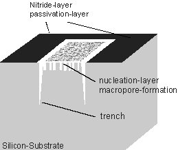
In the present work, p-type silicon with prestructured Si3N4 mask was used.
As a surprising result, a new kind of "pore" (actually a two-dimensional structure dubbed "trench") was observed. The results will be discussed in terms of the "current burst" model [11].
On p-type Si wafers (10 – 20 Wcm, (100) orientation) nitride layers with varying thickness were deposited with a standard PECVD process and structured with standard lithographic processes. Pore etching was performed in an electrochemical cell. A computer controlled all parameters of the measurement setup. The temperature of the electrolyte was constant at 20°C. The electrolyte consisted of 4 wt.-% HF in organic dimethylformamide (DMF). Galvanostatic experiments with current densities between 0.1 and 10 mA/cm2 were performed. In an additional series of experiments, n-type-silicon wafers (10 – 20 Wcm, (100)-orientation) were etched potentiostatically (2 – 18 Volt) under computer-controlled back-side-illumination in the same experimental setup. The valence of the etching process was measured via the mass loss (Dm ) according to the formula:
![]() (1)
(1)
with I =etching current, t=etching
time, Ar=(28,08 g/mol) and Na
=(![]() mol-1).
mol-1).
Some of the etched samples were polished with a diamond-paste to a certain depth to investigate the detailed depth dependence of the pore morphology by SEM.
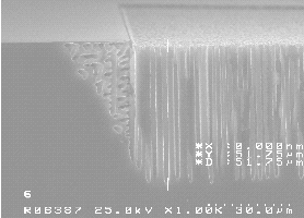
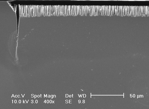
Based on our previous work on macropores on p-type-silicon etched under optimized growth conditions, we studied in particular the underetching of the macropores at the edge of the nitride-layer. Macropores on p-type-silicon grow anisotropically in <100>- and <113>-directions [12], and this behaviour governs the geometry of the underetching. Fig. 1a) shows a SEM micrograph of macropores etched with a current density of 2 mA/cm2 for the free silicon surface, a relatively high degree of underetching of the nitride mask occurs under these conditions.
 |
 |
| Fig. 1a) Cross-section, SEM-micrograph: Macropore-formation at the free silicon surface with a high degree of underetching of the mask. | 1b) Plane-view, SEM-micrograph of the (100)-plane: After polishing off the nitride-mask macropores are clearly visible (and so would be underetching). A significant higher pore-density at the nitride edge is visible. No underetching occurs. |
According to the "current burst model", the current-density employed then must be too high to allow selective pore growth at the macropore tips only, because the average current density that can be carried by all current bursts fitting in the given area in this case is smaller then the externally fixed current density; the system then is forced to nucleate new current bursts even in otherwise unfavorable areas.
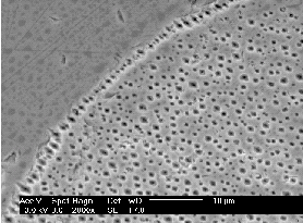
By reducing the current density to 1 mA/cm2, the underetching of the nitride-border is indeed negligible, see Fig. 1b) (in this case the nitride mask was removed because the underetching is always very well visible on plane view samples under the mask). The active areas of the pore-tips are now adequate to drive the externally given current density. Note the higher pore-density at the nitride-border.
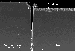
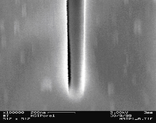
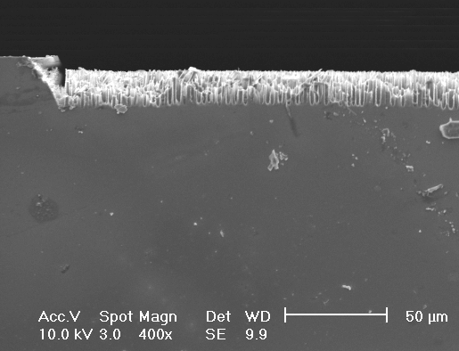
At a further reduction of the current-density a new feature is found (in the following dubbed "trench") which develops from a continuous increase of the diameter and the density of the pores at the nitride edge – see Figs. 2a) and 2b). A schematic outline of the trench is shown in Fig. 2c). The trench formation is connected with a minimal underetch of the nitride mask. The trench grows parallel to the nitride edge on the silicon over large distances (several hundred micrometers have been observed). The trench width is decreasing with the distance from the surface; at the top it is between 1µm – 5µm (tip of the trench with around 70 nm (Fig. 2d)). The growth rate of the trench is 10 µm/min, this is about 10-times higher than the macropore growth rate. The trench grows perpendicular to the surface in <100>-direction (Fig. 2d)).
 |
 |
 |
 |
| Fig. 2a) Cross-section, SEM-micrograph of the (110)-plane: Trench-formation at the border of the nitride layer. The macroporous layer is visible. | b) Plane-view, SEM-micrograph: After polishing the silicon (removing the macropores) the outline of the trench is visible. |
| c) Schematic outline of the trench formation at the edge of the nitride-layer. | d) The tip of the trench has a width of 70 nm. |
The trench formation is induced by a nucleation phase and needs a certain nucleation time. In a first step, the free silicon surface is dissolved relatively homogeneously as observed in other cases (macropores on n- and p-type silicon nucleate with a homogeneous silicon dissolution and surface roughening [13]), and in a second step the trench is formed. In Fig. 2a) the macropore nucleation-layer is visible. After the nucleation, almost all of the current is consumed by the stable trench etching reactions, so the macropores are growing quite slowly.
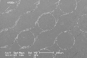
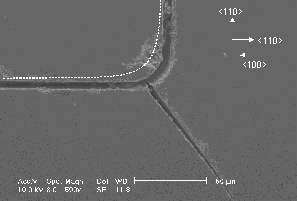
At round mask structures, the trench grows not exactly parallel to the mask border as it gains in depth. The depth dependence of the trench-morphology of the trench has been investigated in detail. In Fig. 3a), following the mask geometry, the trenches start as circles, but straighten out and join up with neighboring trenches with increasing depth (the primarily position of the circular mask is marked by the dotted line). It is evident that the trench prefers to grow anisotropically in <100>-directions, and that this tendency becomes more prominent with increasing depth. Fig. 3b) demonstrates the consequences for a round corner: The trench deviates from the nitride-edge and even a branch no longer connected to the original mask structure is formed in a <100> direction. Obviously the <100> direction is as well the main growth direction for trenches into the depth.
 |
 |
| Fig. 3: Trenches in 30 µm depth; the original mask indicated by dashed lines. a) The trench aligns itself into <100>-directions with increasing depth. |
b) Deviation from round corners and formation of side trenches. |
For technical applications clear design rules for the trench formation and the nitride window can be specified. Mask edges should be oriented along <100>-direction as much as possible for deep and stable trench growth. Round structures should be approximated with <100> oriented saw-tooth structures.
A series of experiments has been performed to investigate the driving force for the trench-formation at the nitride edge. The results imply that the reason for the trench formation at the mask edge is a combination of mechanical stress and electric field effects at the trench tip. A nitride mask is known to induce severe stress in the silicon substrate which depends (linearly) on the mask thickness. A series of experiments with masks of different thickness and an intermediate current density (0.75 mA/cm2; inducing trench as well as macropore formation) was performed. Figs. 4a) and 4b) show the results for two samples: The thicker nitride layer produces a larger trench (Fig. 4a)) in comparison to a thin layer (Fig. 4b)). It thus may be concluded that mechanical stress induces preferential nucleation of current bursts, probably due to stressed bonds. If the H-termination is also affected by stress (which would also change the current burst nucleation probability) is not clear at present.
|
|
 |
|
|
|
| Fig. 4a) A thick nitride-layer (150 nm) produces large trenches. |
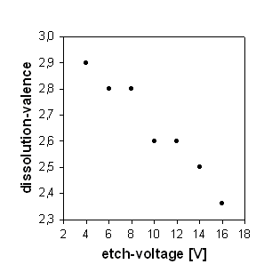
Fig. 4 c) The valence of the silicon dissolution reaction in organic electrolytes measured at n-type-silicon under back-side-illumination and variable voltage is shown. |
| Fig. 4 b) A thin nitride-layer (~ 50 nm) produces no trench at all. |
It is known that the electric field influences the formation of porous silicon [e.g. 14]. In an additional series of experiments, it was attempted to study field strength dependence of the dissolution reaction in organic electrolytes (including DMF) without changing the other parameters. In p-type Si this is not possible because changing the voltage will always change the current, too. Therefore n-type silicon (without a mask) was chosen for this experiment because in this case current and applied voltage can be chosen independently of each other. The
experiments were made at a constant current density (2 mA/cm2, defined by the (controlled) back-side-illumination) and variable external voltages. Besides the pore morphology (reported in [15]), the valence of the dissolution reaction was measured on the base of the mass loss according to equation (1). The results appear applicable to the case of p-type Si and are shown in Fig. 4c). An increasing voltage leads to a decreasing valence. This means that more Si dissolves at higher voltages or field strength for a given current-time product, and that the oxidizing part of the reaction decreases relative to the direct dissolution mechanism. In the context of the current burst model this to be expected (cf. [16]) because with increasing potential the relation between the (constant) concentration of available holes and the concentration of holes that could be consumed by oxidation decreases and the system favors direct dissolution following the principle of maximum power (cf. [16]). Since direct dissolution is strongly anisotropic favoring <100> directions, trench formation is more stable at high field strength. It now can be argued that electrical field strength and mechanical stress will only enhance dissolution where the direct dissolution component is dominant because in the reverse case (oxidation dominates), the oxide layer formed will (i) contain a large part of the potential drop and thus reduce the electric field within the silicon; and (ii) the amorphous oxide layer might serve as a buffer for the mechanical stress, reducing the probability of forming e.g. microcracks as a starting point for enhanced silicon dissolution. In a sense, trench formation could have some relation to the general phenomena of stress corrosion cracking.
With etching parameters optimized by following guidelines of the current burst model [12], macropores can be produced in mask-limited areas without severe underetching of the mask. The basic requirements are:
i) Well developed, smooth macropores with a strong
anisotropy in the <100> growth directions.
ii) Very low nucleation probabilites on H-terminated surfaces, especially on
the pore walls, despite the availabilty of carriers for the outermost pores.
iii) Optimized current=natural current of current bursts fitting in the
available area.
iv) Optimized nucleation; ideally controlled by in-situ impedance analysis
[17].
At the same time a new etch feature, called "trench" has been discovered which provides novel ways for microstructuring Si substrates and offers new insights into the etching mechanisms in Si. The formation conditions for trenches can be generally understood within the current burst model along the following lines: The organic solutions suppresses the anodic oxide formation, the intrinsically anisotropic direct silicon dissolution dominates. Mechanical stress together with an enhancement of the electric field at the trench tip leads to a strongly increased probability for current burst nucleation (overcoming of the H-termination) parallel to the nitride edge and thus to a self amplifying process.
We thank the ISIT (Fraunhofer Institute for Silicon Technology in Itzehoe), especially B. Wagner and A. Heuberger, for structuring the silicon samples and helpful discussions. This work was supported by the Deutsche Forschungsgemeinschaft (Förderungsnummer: FO 258/1-2).
[2] A. G. Cullis, L.T. Canham, P. D. J. Calcott, J. Appl. Phys., 82 (3) (1997)
[3] S. Ottow, V. Lehmann, H. Föll, J. Electrochem. Soc., 143, 385 (1996)
[4] P. Kleinmann, J. Linnros, S. Petersson, Materials Science and Engineering B, 69 - 70 (proceedings of the E-MRS 1999) in press
[5] R. Angelucci, A. Poggi, L. Dori, A. Tagliani, G. C. Cardinali, F. Corticelli, M. Madisaldi, "Permeated Porous Silicon suspended Membrane as sub-ppm Benzene Sensor for Air Quality Montoring" in Proceedings of the Porous Science and Technology Conf., in press (1998)
[6] K. Imai, Solid State Electron., 24, 159 (1981)
[7] F. Müller, A. Birner, U. Gösele, V. Lehmann, S. Ottow, H. Föll, Journal of Porous Materials, 7, 201 – 204 (2000)
[8] V. Lehmann, H. Föll, J. Electrochem. Soc., 137, 653 (1990)
[9] V. Lehmann, U. Grüning, Thin Solid Films, 297, 13-17 (1997)
[10] W. Lang, Silicon microstructuring technology, Materials Science and Engineering, 1, R 17, (1996)
[11] J. Carstensen, M. Christophersen, H. Föll, Materials Science and Engineering B, 69 - 70, 23-28 (2000)
[12] M. Christophersen, J. Carstensen, A. Feuerhake, H. Föll, Materials Science and Engineering B, 59 - 70, 194 (2000)
[13] M. H. Al Rifai, M. Christophersen, S. Ottow, J. Carstensen, H. Föll, J. Electrochem. Soc., 147 (2), 627 (2000)
[14] A. Zeitschel, A. Friedberger, W. Welser, G. Müller, Sensors and Actuators, 74, 113-117 (1999)
[15] M. Christophersen, J. Carstensen, H. Föll, this proceedings
[16] J. Carstensen, M. Christophersen, G. Hasse, H. Föll, this proceedings
[17] G. Hasse, M. Christophersen, J. Carstensen, H. Föll, this proceedings