Formation of porous layers with different morphologies
during anodic etching of n-InP
S. Langa,1,2 I. M. Tiginyanu,2 J.
Carstensen,1 M. Christophersen1, H.
Föll,1
2 Faculty of Engineering, Christian-Albrechts-University,
Kaiserstr. 2, D-24143 Kiel, Germany
2Laboratory of Low-Dimensional Semiconductor Structures,
Institute of Applied Physics, Technical University of Moldova, Stefan cel Mare
168, MD-2004, Chisinau, Moldova
Two different morphologies of porous layers were observed in (100)-oriented n-InP anodically etched in an aqueous solution of HCl. At high current density (60 mA/cm2) anodization leads to the formation of so-called current-line oriented pores. When decreasing the current density to values lower than 5 mA/cm2 the morphology of the porous layers sharply changes and the pores begin to grow along definite <111> crystallographic directions.
While considerable research efforts are focussed to porous Si 1 and silicon-electrolyte junctions,2 relatively little attention has been paid to porous layer morphology in III-V compounds. Pore formation has been reported for InP in HCl,3-6 GaP in H2SO4 electrolytes,7 for GaAs in HCl and Cl- containing solutions.8,9
According to preliminary investigations, the type and concentration of anions in the electrolyte,8,9 as well as the substrate type,10 orientation 10,11 and doping 12,13 are the main parameters significantly affecting the pore growth and morphology in different semiconductor materials. Apart from that, the so-called nucleation phase of pore formation is affected by native or intentionally induced defects on the semiconductor surface. Thus, Tiginyanu et al. reported that preliminary MeV-ion implantation in GaP can serve as a tool for controlling the morphology of pores. 14
The present paper reports on a radical change in pore morphology in n-InP substrates without using additional treatment before or during the anodization.
Wafers used in this work were (100)-oriented n-type InP, doped with Si. The concentration of free electrons in bulk material was 3´ 1017 cm-3 at 300 K. The anodization was carried out in an electrochemical double cell as shown in Figure 1.
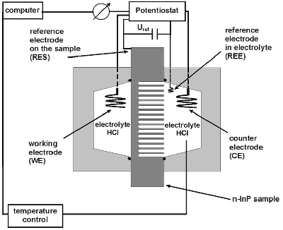 |
Figure 1. Schematic illustration of the electrochemical double cell. |
A four electrode configuration was used: a Pt reference electrode in the electrolyte (REE), a Pt reference electrode on the sample (RES), a Pt counter electrode (CE) and a Pt working electrode (WE). The electrodes were connected to a Keithley 236 Source Measure Unit. The temperature of the electrolyte was kept constant at T=23 oC with the help of a Julabo F25 thermostat only on that side of the double cell where pores were expected to grow. The electrolyte was pumped in a continuous mode through both cells with the help of a peristaltic pump. The equipment involved in the experiments was computer controlled. The area of the sample exposed to the electrolyte was 0.12 cm2. The anodic etching was carried out using 5 % HCl aqueous electrolyte at different galvanostatic conditions. The anodized wafers have been investigated with a Scanning Electron Microscope (SEM) in cross section. Additionally it is important to mention that the experiments have been carried out in the dark and the holes necessary for the dissolution of the material were generated by the breakdown of the depletion layer.
Figure 2 presents the cross section micrograph of a sample anodized at the current density 60 mA/cm2. Pores obtained in these conditions evidently have no specific crystallographic orientation but simply follow some curved lines mainly oriented perpendicular to the surface. The system seems to minimise the ohmic loses by optimising the way for the current.15 Such pores we call "current-line oriented".
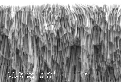 |
Figure 2. SEM micrograph in cross section of a sample subjected to anodic etching at current density 60 mA/cm2. |
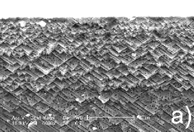
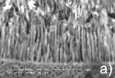
At identical conditions except for a decrease of the anodic current density of more than an order of magnitude, a totally different morphology is obtained (Figure 3). In this case the pores prove to be strictly oriented along specific crystallographic directions. As illustrated in Figure 3, in the cross section of the anodized sample two kinds of pores (trenches and pits) are easily distinguishable. The trenches in the cross section plane are oriented in two different directions intersecting at 108o (54o with the surface normal). This suggests that the pores grow along <111> crystallographic directions. It has to be noted that <111> directions were reported earlier as preferential directions of pore growth in GaAs.12
 |
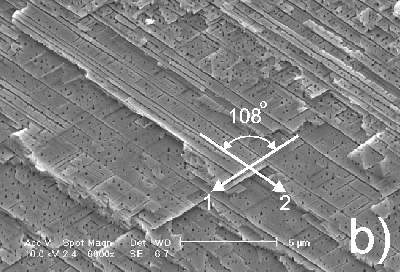 |
Figure 3. Cross section micrograph of n-InP anodized at current density 4.2 mA/cm2 for 2 hours: a) upper part of the porous layer; b) porous layer in depth; the arrows show two preferential directions of pore growth, as described in the text. |
|
The analysis of the images in Figure 3 shows that in the cross section plane two directions of growth are visible as trenches while the other two, not contained in the cleavage plane, appear as pits. According to the SEM images taken at high magnifications, these pits possess a triangular shape. Thus, formation of triangular pores introduces a second anisotropy of the electrochemical etching in InP additional to the preferential direction of growth in <111>.
As can be observed from Figure 3b, along the direction marked on the micrograph with the symbol "2" the pores are rather long and predominant in comparison with the pores which are growing in the direction marked with the symbol "1". Figure 3b looks somehow unsymmetrical taking into the account that these directions ("1" and "2") are crystallographically identical. However, it is important to mention that Figure 3a represents the cross section taken from the upper part of the porous layer, while Figure 3b represents the same porous layer at a larger depth. As one can see, in the upper part of the porous layer the cleavage contains a succession of planes forming a step like structure revealing relatively long pores in both directions. So, in both directions long pores are present, but in a specific cross section plane only one direction may show long pores while in other cross section planes pores with other direction of growth from the same <111> set are predominant.
Taking into account that the results described above are reproducible, one can conclude that a gradual change of current density from low to high values leads to a switch of the pore growth mechanism from being crystallographically oriented to current-line oriented. This conclusion is supported by the images presented in Figure 4. The same n-InP sample was subjected to anodization first at high, and then at low current densities. As can be seen in the cross section of the sample, a switch occurs from the current-line oriented to the crystallographically oriented pores. The upper part of the porous layer has a current-line oriented morphology and corresponds to high current density (Figure 4a), while the lower part of the layer contains crystallographically oriented pores (Figure 4b).
 |
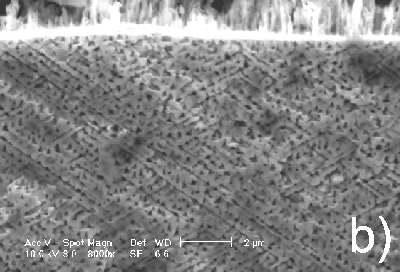 |
Figure 4. Cross section micrographs of n-InP anodized in turn at high and low current densities (60 and 5 mA/cm2, respectively): a) upper part of the porous layer; b) porous layer in depth. |
|
In spite of the fact that the current-line oriented pores grow preferentially perpendicular to the surface they show a pronounced instability in their direction of growth (see for example Figure 2). One of the main reasons of this instability appears to be the difference between the preferential crystallographic direction of growth (<111> directions) and the direction of current-line oriented pores, i.e., [100] direction in our case. This difference may act as a destabilising factor for the direction of growth for current-line oriented pores.
It is noteworthy to mention that the instability of the direction of pore growth at high current densities is more pronounced when the anodic current through the sample is applied in pulses, this means that the current is also a factor influencing the direction of growth for the current-line oriented pores.
In conclusion, anodic etching of n-InP in HCl based electrolyte at high current densities leads to the orientation of pores along the current lines, while anodization at low current densities provide conditions for preferential orientation of pores along four <111> crystallographic directions. When applied via lithographically defined windows, the etching of n-InP at low anodic current densities may be used to produce ordered three dimensional structures promising for photonic applications.16 This issue is under investigation in our laboratories.
2. H. Föll, Appl. Phys. A, 53, 8, (1991).
3. N.G. Fereira, D. Soltz, F. Decker, and L. Cescato, J. Electrochem. Soc., 142, 1348 (1995).
4. T. Takizawa, S. Arai, M. Nakahara, Jap. J. Appl. Phys., 54, L643 (1994).
5. E. Kikuno, M. Amitti, T. Takizawa, S. Arai, Jpn. J. Appl. Phys., 34, 177 (1995).
6. A. Hamamatsu, C. Kaneshiro, H. Fujikura, H. Hasegawa, J. Electroanal. Chem., 473, 223 (1999).
7. B.H. Erne, D. Vanmeakelbergh, and J.J. Kelly, J. Electrochem. Soc., 143, 305 (1995).
8. P. Schmuki, J. Fraser, C.M. Vitus, M.J. Graham, and H. Isaacs, J. Electrochem. Soc., 143, 3316 (1996).
9. P. Schmuki, D. J. Lockwood, J. W Fraser, M.J. Graham, and H. Isaacs, Mater. Res. Soc. Symp. Proc., 431, 439 (1996).
10. M. Christophersen, J. Carstensen, A. Feuerhake, and H. Föll, Mat. Sci. Eng., B, 69-70, 194, (2000).
11. S. Rönnebeck, J. Carstensen, S. Ottow, and H. Föll, Electrochem. Solid-State Lett., 2, 126, (1999).
12. F.M. Ross, G. Oskam, P.C. Searson, J.M. Macaulay, and J.A. Liddle, Philosophical Magazine A, 75, 2, (1997).
13. P. Schmuki, L.E. Erickson, D.J. Lockwood, J.W. Fraser, G. Champion, H.J. Labbe, Appl. Phys. Lett., 72, 1039, (1998).
14. I. M. Tiginyanu, C. Schwab, J.-J. Grob, B. Prevot, H.L. Hartnagel, A. Vogt, G. Irmer and J. Monecke, Appl. Phys. Lett., 71, 26, (1997).
15. G.S. Popkirov, R.N. Schindler, Electrochim Acta, 39, 2025 (1994).
16. F. Müller, A. Birner, U. Gösele, V. Lehmann, S. Ottow, and H. Föll, J. Por. Mat., 7, 201, (1998).