DEEP ELECTROCHEMICAL TRENCH ETCHING WITH ORGANIC
HYDROFLUORIC ELECTROLYTES
M. Christophersen (a), P. Merz (a), J. Quenzer (b), J.
Carstensen (a), and H. Föll (a)
(a) Materials Science, Faculty of Engineering
Kaiserstrasse 2, 24143 Kiel, Germany
Phone: + 49 431 77572-501, Email: hf@tf.uni-kiel.de
(b) Fraunhofer Institute for Silicon Technology
Fraunhoferstraße 1, 25524 Itzehoe, Germany
Porous silicon layers etched through openings in an inert masking layer have potential applications for producing microstructures in silicon. In order to overcome the isotropic nature of the porous silicon formation process around the mask edges, optimized organic electrolytes for etching macropores on p-type silicon were employed. New kind of pores (dubbed "trenches") were found, which are sensitive to mechanical stress and may prove useful for microstructuring silicon. Systematic experiments are presented which investigate the stability, the crystal orientation dependence, and limitations of trench formation.
Electrochemical etching; p-type silicon; Trench structure; Macropores
Microporous silicon has attracted a great deal of attention due to its interesting light emission properties [e.g. 1, 2]. A different line of research investigated the use of porous Si layers (PSL) for microstructuring of Si [3 - 10]. Nanoporous PSL may also be used as a sacrificial layer, e.g. for SOI devices [11, 12]. Ottow et. al. [3] developed a complete process for three dimensional microstructuring using macroporous n-type silicon which was used, e.g., for the production of photonic crystals [13]. This process is based on the macropore formation on n-type silicon in diluted hydrofluoric acid [14, 15]. In 1990 Lehmann and Föll [14] discovered that very regular arrays of macropores with extremely large aspect ratios could be obtained in the n-Si/HF system. Lehmann et. al. [16] developed a technique for capacitor fabrication on n-type macoporous silicon. Ohji et. al. [7] were able to build free standing silicon structures based on macroporous silicon on n-type silicon and trench structures in p-type silicon [10] using an electrochemical etching. In a recent review [17], the major ways of silicon micro-machining technologies were compared, including anisotropic silicon etching and using porous silicon layers.
In 1994 macropores on p-type silicon were found by Propst and Kohl [18] by anodic etching in a HF containing organic electrolyte (HF in water free acetonitril). In the following years, several papers were published dealing with macropores on p-type Si [19 - 22] and their possible formation mechanism. It is practicable to etch macropores in p-type silicon by using optimized organic electrolytes with better aspect ratios, better stability, and smaller diameters in comparison to n-type macropores [22]. Another advantage of using p-type silicon for macropore formation is that no illumination of the silicon sample is necessary. In the present paper we extend our previous work on p-type silicon macropores [22] using p-type silicon samples with prestructured Si3N4 mask. As a surprising result, a new kind of "pore" (actually a two-dimensional structure dubbed "trench") was observed.
On p-type Si wafers (10 – 20 Wcm, (100) orientation) nitride layers with varying thickness were deposited with a standard PECVD process and structured with standard lithographic processes. KOH pits were chemically etched. It has been shown that KOH pits can be used as starting points for macropores on p- [21] and n-type silicon [15]. The free silicon surfaces were defined with the nitride windows for etching random p-type macropores [23] and arrays of pits for prestructured macropores. Pore etching was performed in an electrochemical cell (etch area 1 cm2). A computer controlled all parameters of the measurement setup. The temperature of the electrolyte was constant at 20°C. The electrolyte consisted of 4 wt.-% HF (from a 48 wt.-% solution) in organic dimethylformamide (DMF). Galvanostatic experiments with current densities between 0.1 and 10 mA/cm2 were performed. Some of the etched samples were polished with a diamond-paste to different depths to investigate the detailed depth dependence of the pore morphology by SEM.
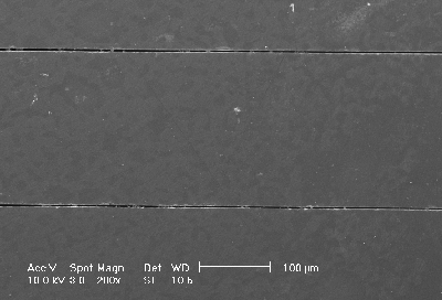
With the KOH-pits the macropore nucleation can be defined. Fig. 1 shows a SEM micrograph in plane-view: Arrays of macropores can be seen – the pores were etched galvanostatically at 1.5 mA/cm2 (relating to the free silicon surface). The nitride layer was chemically removed and 10 µm of the silicon surface were polished off to study the uniformity of the p-type macropore formation in the depth. When the macropores reaches a depth over 20 µm the macropores at the outside of the array begin to growth faster than the rest. This may be caused by the same effects with lead to the "trench" formation. The trench formation will be discussed in detail below – the trend for the current density dependence is the same for prestructured macropore nuclei and free silicon surfaces.
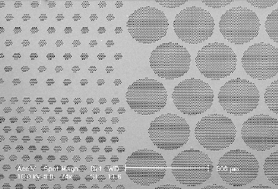 |
Fig. 1) Plane-view, SEM micrograph of the (100)-plane: Arrays of p-type macropores were etched on prestructured silicon. The nitride layer was chemical removed and 10 µm of the silicon surface were polished off to study the uniformity of the p-type macropore formation in the depth. |
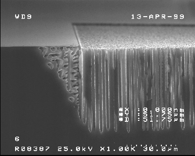
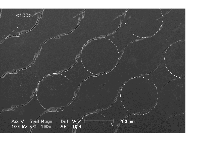
Based on our previous work on random macropores on p-type silicon etched under optimized growth conditions, we studied in particular the underetching of the macropores of free silicon surfaces at the edge of the nitride-layer. Macropores on p-type silicon grow anisotropically in <100>- and <113>-directions [22, 24], and this behavior governs the geometry of the underetching at free silicon surfaces. Fig. 2a) shows a SEM micrograph of macropores etched with a current density of 2 mA/cm2 for the free silicon surface, a relatively high degree of underetching of the nitride mask occurs under these conditions.
 |
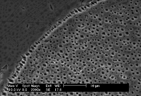 |
Fig. 2a) Cross section, SEM micrograph: Macropore formation at the free silicon surface with a high degree of underetching of the mask. |
2b) Plane view, SEM micrograph of the (100)-plane: After polishing off the nitride mask macropores are clearly visible (and so would be underetching). A significant higher pore density at the nitride edge is visible. No underetching occurs. |
The degree of underetch can be reduced by decreasing the current density. If combining all observations relating to macropore formation (including the orientation and electrolyte dependence of macropore formation on p- and n-type Si [22, 25]), we are led to believe that the silicon dissolution at the macropore tip is spatially and temporally inhomogeneous [26] ("current burst model") – an introduction to the current-burst model is given in [27, 28]. According to the "current burst model" [26], the current density employed therefore must be too high to allow selective pore growth at the macropore tips only, because the average current density that can be carried by all current bursts fitting in the given area in this case is smaller then the externally fixed current density; the system then is forced to nucleate new current bursts even in otherwise unfavorable areas.
By reducing the current density to 1 mA/cm2, the underetching of the nitride border is indeed negligible, see Fig. 2b) (in this case the nitride mask was removed because the underetching is always well visible on plane view samples under the mask). The active areas of the pore tips are now adequate to drive the fixed current density. Note the higher pore density at the nitride border.
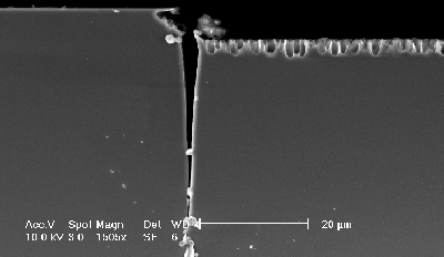
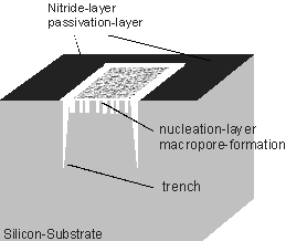
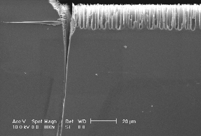
At a further reduction of the current density a new feature is found (in the following dubbed "trench") which develops from a continuous increase of the diameter and the density of the pores at the nitride edge – see Figs. 3a) and 3b). A schematic outline of the trench is shown in Fig. 3c). The trench formation is connected with a minimal underetch of the nitride mask. The trench grows parallel to the nitride edge on the silicon over large distances (several hundred micrometers have been observed). The trench width is decreasing with the distance from the surface; at the top it is between 1µm – 5µm (tip of the trench with around 70 nm (Fig. 3d)). The growth rate of the trench is 10 µm/min, this is about 10-times higher than the macropore growth rate (these are much higher growth rates then reported in [10]). The trench grows perpendicular to the surface in <100>-direction (Fig. 3d)).
 |
 |
 |
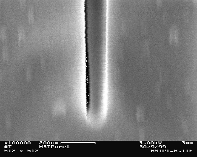 |
Fig. 3a) Cross-section, SEM-micrograph of the (110)-plane: Trench-formation at the border of the nitride layer. The macroporous layer is visible. |
b) Plane-view, SEM-micrograph: After polishing the silicon (removing the macropores) the outline of the trench is visible. |
c) Schematic outline of the trench formation at the edge of the nitride layer. |
d) The tip of the trench has a width of 70 nm. |
The trench formation is induced within a nucleation phase and needs a certain nucleation time. In a first step, the free silicon surface is dissolved relatively homogeneously as observed in other etching conditions as well (macropores on n- and p-type silicon nucleate by a homogeneous silicon dissolution of the surface, which leads to a surface roughening [22, 23]), and in a second step the trench is formed. In Fig. 3a) the macropore nucleation layer is visible. After the nucleation almost all of the current is consumed by the stable trench etching reactions. The macropores stops growing.
At round mask structures, the trench grows not exactly parallel to the mask border as it gains in depth. The depth dependence of the trench morphology of the trench has been investigated in detail. In Fig. 4a), following the mask geometry, the trenches start as circles, but straighten out and join up with neighboring trenches with increasing depth (the primarily position of the circular mask is marked by the dotted line). It is evident that the trench prefers to grow anisotropically in <100> directions, and that this tendency becomes more prominent with increasing depth. Fig. 4b) demonstrates the consequences for a round corner: The trench deviates from the nitride edge and even a branch no longer connected to the original mask structure is formed in a <100> direction. Obviously the <100> direction is as well the main growth direction for trenches into the depth.
 |
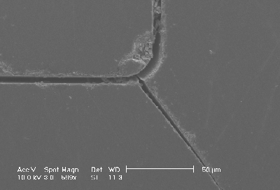 |
Fig. 4): Trenches in 30 µm depth; the original mask indicated by dashed lines. |
|
a) The trench aligns itself into <100>-directions with increasing depth. |
b) Deviation from round corners and formation of side trenches. |
With mask edges parallel to the <100> direction it was possible to etch trenches over several hundred mm lateral on the silicon substrate. Trenches up to 300 mm into the substrate were obtained. On a 1 cm2 sample the reproducibility for the pore depth was better than 5 %. At about 250 mm the trench growth rate is decreasing and the macropores are starting to grow simultaneously into the substrate. This may be an effect of diffusion limitation for the chemical species of the electrochemical reaction into the trench, or the driving forces (discussed below) become weaker with increasing trench depth. So very deep trenches with a depth up to the wafer thickness (~ 500 µm) are a great challenge. For larger structures (> 100 µm) the bending of the trench tips is not so important; so with some effort such structures could probably be etched completely through the wafer.
For technical applications some rules for the trench formation and the nitride window can be specified. Mask edges should be oriented along <100> directions as much as possible for deep and stable trench growth. Round structures should be approximated with <100> oriented "saw"-tooth structures. The interaction between two neighboring trenches must be studied in more details, but it is quite obvious that the smallest allowed distance between not interacting trenches scales with the depth of the trenches. For trenches deeper than 100 µm the width of the nitride windows between two trenches should at least be in the range of about 50 µm.
A series of experiments has been performed to investigate the driving force for the trench formation at the nitride edge. The results imply that the reason for the trench formation at the mask edge is a combination of mechanical stress and electric field strength effects at the trench tip. A nitride mask is known to induce severe stress in the silicon substrate which depends (nearly linearly) on the mask thickness. A series of experiments with masks of different thickness and an intermediate current density (0.75 mA/cm2; inducing trench as well as macropore formation) was performed. Figs. 5a) and 5b) show the results from two samples: The thicker nitride layer produces a larger trench (Fig. 5a)) in comparison to a thin layer (Fig. 5b)). It thus may be concluded that mechanical stress induces preferential electrochemical silicon dissolution, probably due to stressed bonds. This experimental results show that for stable p-type macropore etching using organic electrolytes [e.g. shown in 10] a mask should be used which is not introducing stress into the silicon substrate.
 |
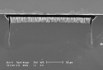 |
Fig. 5a) A thick nitrid layer (150 nm) produces large trenches. |
b) A thin nitride layer (~ 50 nm) produces no trench at all. |
It is known that the electric field influences the formation of porous silicon [e.g. 23]. Zeitschel et. al. used this feature to design mircostructured silicon [6] – they obtained smooth gradients in microporous silicon with applying an inhomogeneous electric field. In an additional series of experiments on n-type Si [presented in 25] (in p-type Si this is not possible because changing the voltage will always change the current, too), it was attempted to study field strength dependence on the dissolution reaction in organic electrolytes (including DMF) without changing the other parameters: Silicon is easier dissolved by applying a higher electric field strength. In a sense, trench formation could have some relation to the general phenomena of stress corrosion cracking, which is in fact so far unknown for electrochemical silicon etching with hydrofluoric acid containing electrolytes (so it is a totally different etch mechanism in comparison to the trench formation presented in [10]).
Trench formation needs all three components: mechanical stress, applied potential, and chemical reactions. It is not only a chemically enhanced crack, since no trench is found if no potential is applied. The fact that the trench formation is indeed an electrochemical process increases the degrees of freedom for pore formation in comparison to a purely chemical etching: The silicon dissolution reactions and thus the trench formation can be changed strongly by the composition of the electrolyte (e.g. solvent, HF concentration) and independently by the applied electric field. So optimizing the Si doping, the nitride thickness, the electrolyte, and the potential trenches with well reproducible width and depth can be formed at least on small Si samples.
The great challenge for applications is the implementation of electrochemical Si etching on large (e.g. 6 inch) wafers. The reproducibility of trench formation (and other Si pores) depends essentially on the homogeneity of the electric back contact and a homogenous electrolyte flow across the wafer. Getting some experiences with a 6 inch electrochemical etching cell we believe that it is possible to achieve as good reproducibility for the trench etching on a large wafer as on our 1 cm2 samples.
At this state complicating micromechanical structures can not be realized with trenches. But large holes (> 100 µm diameter) may be etched even through the complete wafer which would allow for the wiring of devices on the backside of the wafer.
With etching parameters optimized, macropores on p-type silicon can be produced in mask limited areas without severe underetching of the mask. KOH pits are suitable to prestructure the macropore formation in certain areas on the substrate. At the same time a new etch feature, called "trench" has been discovered which provides novel ways for microstructuring Si substrates. The formation conditions for trenches can be generally understood as a local enhanced direct silicon dissolution: The organic solutions suppress the anodic oxide formation, therefore the intrinsically anisotropic direct silicon dissolution dominates. Mechanical stress together with an enhancement of the electric field at the trench tip leads to a strongly increased probability for the electrochemical silicon dissolution parallel to the nitride edge and thus to a self amplifying process of the Si dissolution. A trench with lateral width up to several hundred mm – trench depths up to 300 into the silicon substrate was realized. The trench tip is very small – the minimal width is down to 70 nm. The width of the trench can be varied by the nitride window with limits (from ~ 100 nm up to several micrometers). The trench formation process is very fast and anisotropic in <100> direction and is a new technique for silicon structuring.
We thank the ISiT (Fraunhofer Institute for Silicon Technology in Itzehoe), especially B. Wagner and A. Heuberger, for structuring the silicon samples and helpful discussions. This work was supported by the Deutsche Forschungsgemeinschaft (Förderungsnummer: FO 258/1-2).
[2] R. L. Smith, S. D. Collins, Porous silicon formation mechanism, J. Appl. Phys. 71 (8) (1992) R1-R22
[3] S. Ottow, V. Lehmann, H. Föll, Processing of three-dimensional microstructures using macroporous n-type silicon, J. Electrochem. Soc. 143 (1996) 385-390
[4] P. Kleinmann, J. Linnros, S. Petersson, Formation of wide and deep pores in silicon by electrochemical etching, Materials Science and Engineering B69 - 70 (2000) 29-30
[5] R. Angelucci, A. Poggi, L. Dori, A. Tagliani, G. C. Cardinali, F. Corticelli, M. Madisaldi, Permeated porous silicon suspended membrane as sub-ppm benzene sensor for air quality montoring, Journal of Porous Materials 7(1/3) (2000) 197-200
[6] A. Zeitschel, A. Friedberger, W. Welser, G. Müller, Breaking the isotropy of porous silicon formation by means current focusing, Sensors and Actuators 74 (1999) 113-117
[7] H. Ohji. P.J. Frebch, Single step electrochemical etching in ammonium fluoride, Sensors and Actuators 74 (1999) 109-112
[8] H. Artmann, W. Frey, Porous silicon technique for realization of surface micromachined silicon structures with large gaps, Sensors and Actuators 74 (1999) 104-108
[9] H. Ohji, P. J. Trimp, P. J. French, Fabrication of free standing structure using single step electrochemical etching in hydrofluoric acid, Sensors and Actuators 73 (1999) 95 – 100
[10] H. Ohji, P. J. French, K. Tsutsumi, Fabrication of mechanical structures in p-type silicon using electrochemical etching, Sensors and Actuators 82 (2000) 254-258
[11] K. Imai, A new dielectric isolation method using porous silicon, Solid State Electron. 24 (2) (1981) 159-163
[12] T. Yonehara, ELTRAN ®; SOI-Epi Wafer ® and SCLIPS by epitaxial layer transfer from porous silicon, Proceedings of the 2nd Int. Conf. of Porous Semiconductor Science and Technology (2000) to be published
[13] F. Müller, A. Birner, U. Gösele, V. Lehmann, S. Ottow, H. Föll, Structuring of macroporous silicon for applications as photonic crystals, Journal of Porous Materials 7(1/3) (2000) 201-204
[14] V. Lehmann, H. Föll, Formation mechanism and properties of electrochemically etched trenches in n-type silicon, J. Electrochem. Soc. 137 (2) (1990) 653-658
[15] V. Lehmann, U. Grüning, The limits of macropore array fabrication, Thin Solid Films 297 (1997) 13-17
[16] V. Lehmann, W. Hönlein, H. Reisinger, A. Spitzer, H. Wendt, J. Willer, A novel capacitor technology based on porous silicon, Thin Solid Films 276 (1-2) (1996) 138-142
[17] W. Lang, Silicon microstructuring technology, Materials Science and Engineering 1 (1996) R17 – R25
[18] E. K. Propst, P. A. Kohl, The electrochemical oxidation of silicon and formation of porous silicon in acetonitrile, J. Electrochem. Soc.141 (4) (1994) 1006-1013
[19] E. A. Ponomarev, C. Levy-Clement, Macropore formation on p-type Si in fluoride containing organic electrolytes, J. Electrochem. Soc. Lett. 1, (1998) 42-45
[20] R. B. Wehrspohn, F. Ozanan, J.-N. Chazalviel, Macropore formation in highly resistive p-type crystalline silicon, J. Electrochem. Soc. 145 (8) (1998) 2958-2960
[21] V. Lehmann, S. Rönnebeck, The physics of macropore formation in low-doped p-type silicon, J. Electrochem. Soc. 146 (8) (1999) 2968-2975
[22] M. Christophersen, J. Carstensen, A. Feuerhake, H. Föll, Crystal orientation and electrolyte dependence for macropore formation and stable growth on p-type Si, Materials Science and Engineering B59 – 70 (2000) 194
[23] M. H. Al Rifai, M. Christophersen, S. Ottow, J. Carstensen, H. Föll, Dependence of macropore formation in n-Si on potential, temperature, and doping, J. Electrochem. Soc. 147 (2) (2000) 627-635
[24] S. Rönnebeck, J. Carstensen, S. Ottow, H. Föll, Crystal orientation dependence of macropore growth in n-type silicon, Electrochemical and Solid-State Letters 2 (3) (1999) 126-128
[25] M. Christophersen, J. Carstensen, H. Föll, Crystal orientation dependence of macropore formation of p- and n-type silicon, Proceedings of the 2nd Int. Conf. of Porous Semiconductor Science and Technology (2000) to be published
[26] J. Carstensen, M. Christophersen, H. Föll, Pore formation mechanisms for the Si-HF system, Materials Science and Engineering B 69 – 70 (2000) 23-28
[27] H. Föll, J. Carstensen, M. Christophersen, G. Hasse, A new view of silicon electrochemistry, Proceedings of the 2nd Int. Conf. of Porous Semiconductor Science and Technology (2000) to be published
[28] J. Carstensen, M. Christophersen, G. Hasse, H. Föll, Parameter dependence of pore formation in silicon within a model of local current bursts, Proceedings of the 2nd Int. Conf. of Porous Semiconductor Science and Technology (2000) to be published
Marc Christophersen was born in the Federal Republic of Germany 1972. He received the M.Eng. in materials science in November 1998 form the University of Kiel. His diploma work dealt on macroporous n- and p-type silicon. Since January 1999 he is working for his PhD in the group of Prof. Dr. Föll. His main research activity is the development of a model for pore formation in silicon.
Peter Merz was born in Switzerland in1972. He received the M.Eng. in materials science from the University of Kiel in October 1997. His Diploma work dealt with the deposition and characterization of PECVD BPSG. Since January 1999 he has been working towards his PhD in a cooperation project between the group of Prof. Dr. Föll of the University Kiel and the Microsystems Department of the Fraunhofer Institute of Silicontechnology ISIT (Itzehoe). His main research activities are the development and replication of microstructures in different materials.
Hans Joachim Quenzer was born in Bad Mergentheim, Federal Republic of Germany in 1961. He recieved the Dipl.Phys. degree in Physics from the University of Würzburg in 1988. Following the graduation he joined the Fraunhofer Institut für Mikrostrukturtechnik (now the Fraunhofer Institut für Siliziumtechnologie), working in the Microsystems department. Microelectromechanical systems on the basis of silicon technology are in the focus of his work. He is responsible for the development of micromechanical actuators and sensors.
Jürgen Carstensen was born in Flensburg, Federal Republic of Germany in 1964. He received the Dipl. Phys. degree in Physics from the University of Kiel in 1990. Following the graduation he started a Ph.D. thesis on the band structure of high temperature superconductors in the department for theoretical physics in Kiel. After his examination in 1993 he joined the chair for material science of Prof. H. Föll at the technical faculty of the university of Kiel. The electrochemistry of silicon, its theoretical description and technical applications are in the focus of his work.
Helmut Föll was born in Backnang, Federal Republic of Germany, in 1949. After graduating in physics from the university of Stuttgart and PhD work at the Max-Planck-Institut für Metallforschung he worked as a post-doc at the Mat. Science Dept. of Cornell-University and at the T.J. Watson Labs of IBM in Yorktown Heights. 1981 he joined Siemens where he held various positions in solar cell and microelectronic research and development. In 1990 he was appointed the founding dean and full Professor of the new Technical Faculty of the University of Kiel.